Erasing and writing-in circuit and method used for EEPROM (Electrically Erasable Programmable Read-Only Memory)
A technology for writing circuits and memories, applied in static memory, read-only memory, information storage, etc., can solve the problems of low utilization rate of EEPROM storage space, inflexible EEPROM writing data, unusable application occasions, etc., to achieve storage space utilization The effect of high rate, flexible data writing, and fast data writing speed
- Summary
- Abstract
- Description
- Claims
- Application Information
AI Technical Summary
Problems solved by technology
Method used
Image


Examples
Embodiment 1
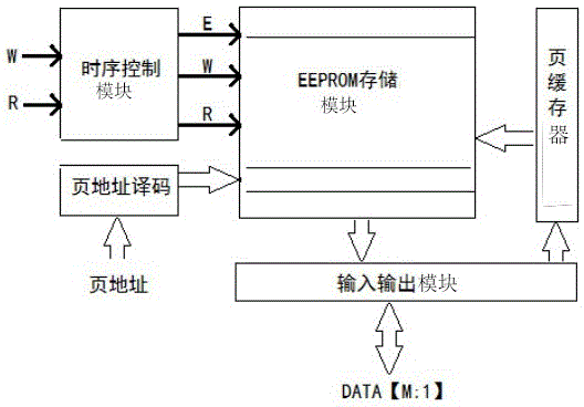
[0028] An erasing and writing circuit for EEPROM memory, comprising: timing control module, storage module, input and output module, page cache module, page address decoder; it is characterized in that, also includes: address decoder in the page , the storage steps are as follows:
[0029] S101, the timing control circuit generates a signal PE after receiving the write signal W;
[0030] S102, the page address decoder decodes and selects the page address to be erased;
[0031] S103, saving the page data to be erased in the page cache;
[0032] S104, the timing control module generates an E signal to erase the page data of the selected page address;
[0033] S105, the byte address decoder in the page decodes and selects the byte address that needs to write data in the page buffer;
[0034] S106, writing the data to be updated into the byte address of the selected page buffer;
[0035] S107, the timing control module generates a W signal, and writes the data in the page buff...
Embodiment 2
[0040] The present invention is used for erasing and writing circuit and method thereof for EEPROM, and its feature is: the mode of erasing data and program writing data of EEPROM memory is the mode of whole page erasing and whole page writing, before erasing data, The erased page data of the EEPROM memory is also read into the page cache, page cache data, page cache data can write "0" or "1", the data to be programmed can be a whole page or a word The data to be programmed is read into the page cache, and then the data in the page cache is programmed to the corresponding page of the EEPROM memory by the whole page.
[0041] When the timing control circuit receives the write signal W, it generates a signal PE to save the page data to be erased in the page cache. That is, the page address of the page data to be erased in the EEPROM memory is decoded by the page address decoder, that is, the page address of the storage unit in the EEPROM memory is selected by the page address de...
PUM
 Abstract
Description
Claims
Application Information