layout-optimized integrated circuits

A technology of integrated circuits and power lines, applied in the field of circuit design, can solve the problems of high cost, achieve the effects of reducing conflicts, reducing the number of metal layers, and reducing costs

Active Publication Date: 2019-03-19
BRITE SEMICON SHANGHAI CORP
View PDF4 Cites 0 Cited by
  • Summary
  • Abstract
  • Description
  • Claims
  • Application Information

AI Technical Summary

Problems solved by technology

exist figure 2 Among them, the packaging pad 110 of the signal unit and the power line and ground line of the lower layer are in the same area. To solve this conflict, the only way to solve this conflict is to increase the number of metal layers. The existing technology generally requires eight or more layers of metal, and the cost is high.

Method used


Image

  • layout-optimized integrated circuits
  • layout-optimized integrated circuits
  • layout-optimized integrated circuits

Examples


Embodiment Construction

[0022] In order to make the above objects, features and advantages of the present invention more comprehensible, the present invention will be further described in detail below in conjunction with the accompanying drawings and specific embodiments.

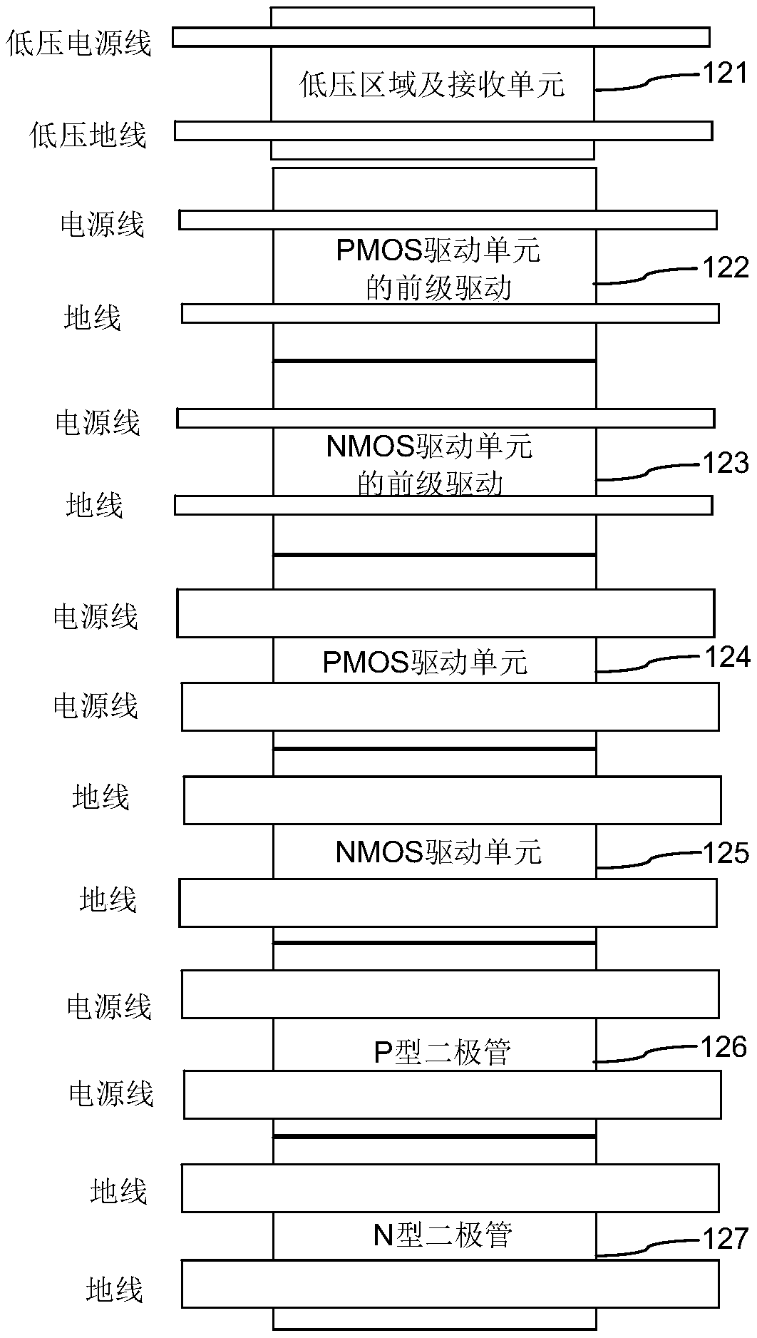
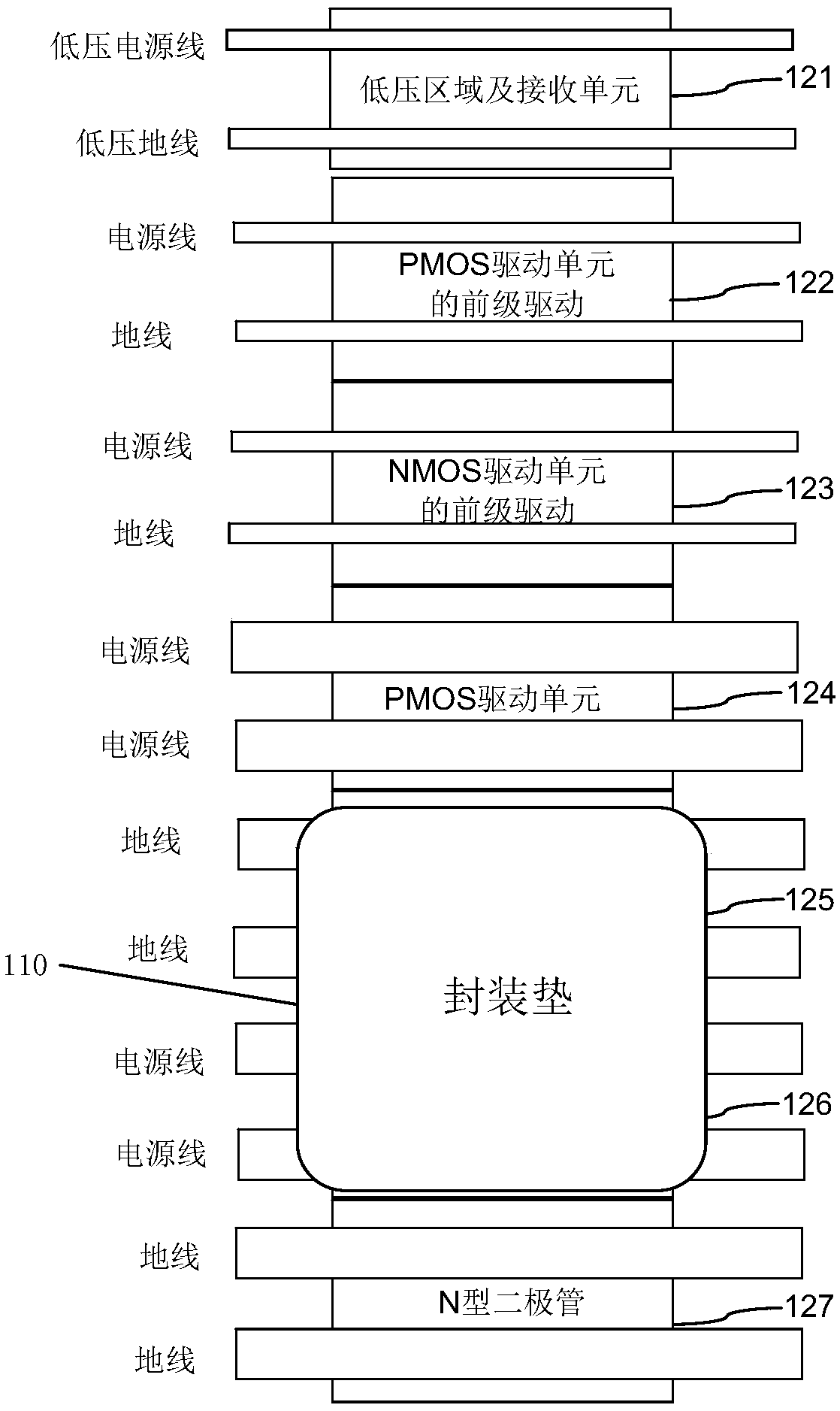
[0023] The present invention changes the layout of the traditional interface unit so that the main power line / ground area in the interface unit is separated from the package pad area, thereby reducing the conflict between the package pad and the power line / ground line in the interface unit, thereby reducing the overall The number of metal layers reduces costs.

[0024] Please refer to image 3 As shown, it is a schematic diagram of the layout layout of the signal unit that does not show the package pad in one embodiment of the present invention; please refer to Figure 4 shown in the image 3 A schematic diagram of the layout layout of the signal unit after adding the package pad in . Depend on image 3 and Figure 4 It can b...


PUM


Abstract

The invention discloses an integrated circuit with optimized layout. The integrated circuit is characterized by comprising a signal unit; the signal unit comprises a packaging pad, a low-voltage area, a receiving unit, a former driver of a PMOS driving unit, a former driver of an NMOS driving unit, the PMOS driving unit, the NMOS driving unit, a P type diode and an N type diode; the P type diode and the N type diode are used for static protection, and the projection area of the packaging pad on a wafer is separated from the projection areas of the PMOS driving unit and the NMOS driving unit on the wafer. According to the integrated circuit, the layout of a traditional interface unit is changed so that a main power line / ground wire area in an interface unit is separated from the packaging pad area; therefore, conflicting between the packaging pad in the interface unit and a power line / ground wire is reduced, then the total number of layers of metal is reduced, and cost is reduced.

Description

【Technical field】 [0001] The invention relates to the field of circuit design, in particular to an integrated circuit with interface unit layout optimization. 【Background technique】 [0002] The layout of the signal interface of the existing DDR (Double Data Rate) 2 / DDR3 / LPDDR2 / LPDDR3 / DDR4 / LPDDR4lvds chips (or integrated circuits, chips) is usually arranged in order from the inside to the outside: low voltage area and receiving Unit 121, the front-stage driver 122 of the PMOS drive unit, the front-stage driver 123 of the NMOS drive unit, the PMOS drive unit 124, the NMOS drive unit 125, the P-type diode 126 and the N-type diode 127 used for electrostatic protection. For details, please refer to figure 1 As shown in FIG. 2 , it is a schematic diagram of the layout layout of signal units without packaging pads in the prior art. The layout requires multiple layers of metal to meet the current requirements (such as figure 1 The power line and ground line shown), each additiona...

Claims


Application Information

Patent Timeline
Patent Type & Authority Patents(China)
IPC IPC(8): H01L27/02
CPCH01L27/0203
Inventor 孔亮季云鹏庄志青职春星
Owner BRITE SEMICON SHANGHAI CORP
Why Eureka
Try Eureka