A positioning reference point and method for improving circuit board cutting accuracy

A positioning reference and positioning method technology, which is applied in the direction of printed circuit, printed circuit manufacturing, printed circuit components, etc., can solve the problems of inaccurate positioning coordinates and affecting cutting accuracy, etc.

Active Publication Date: 2019-04-26
NINGBO SUNNY OPOTECH CO LTD
View PDF5 Cites 0 Cited by
  • Summary
  • Abstract
  • Description
  • Claims
  • Application Information

AI Technical Summary

Problems solved by technology

[0006] An object of the present invention is to provide a positioning reference point and method for improving the cutting accuracy of circuit boards. By setting reference points on the PCB as positioning reference points, it is possible to solve the inaccurate positioning coordinates caused by PCB deformation and expansion and contraction during PCB segmentation. Thus affecting the cutting accuracy problem, in order to ensure the cutting accuracy

Method used


Image

  • A positioning reference point and method for improving circuit board cutting accuracy
  • A positioning reference point and method for improving circuit board cutting accuracy
  • A positioning reference point and method for improving circuit board cutting accuracy

Examples


Embodiment Construction

[0036] The following description is used to disclose the present invention so that those skilled in the art can implement the present invention. The preferred embodiments in the following description are only examples, and those skilled in the art can think of other obvious variations. The basic principles of the present invention defined in the following description can be applied to other embodiments, modifications, improvements, equivalents, and other technical solutions that do not depart from the spirit and scope of the present invention.

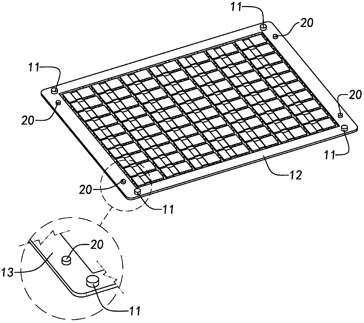
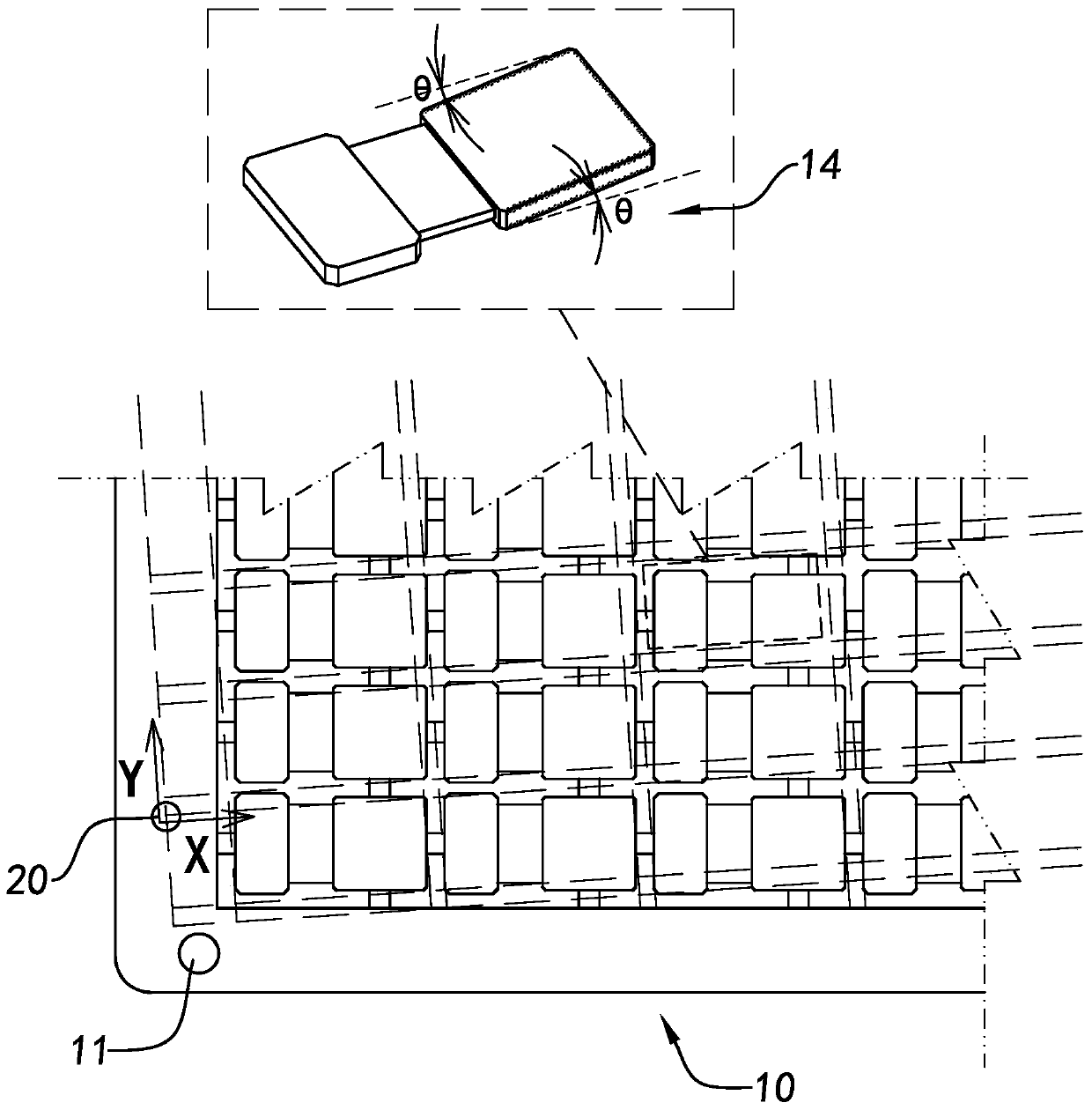
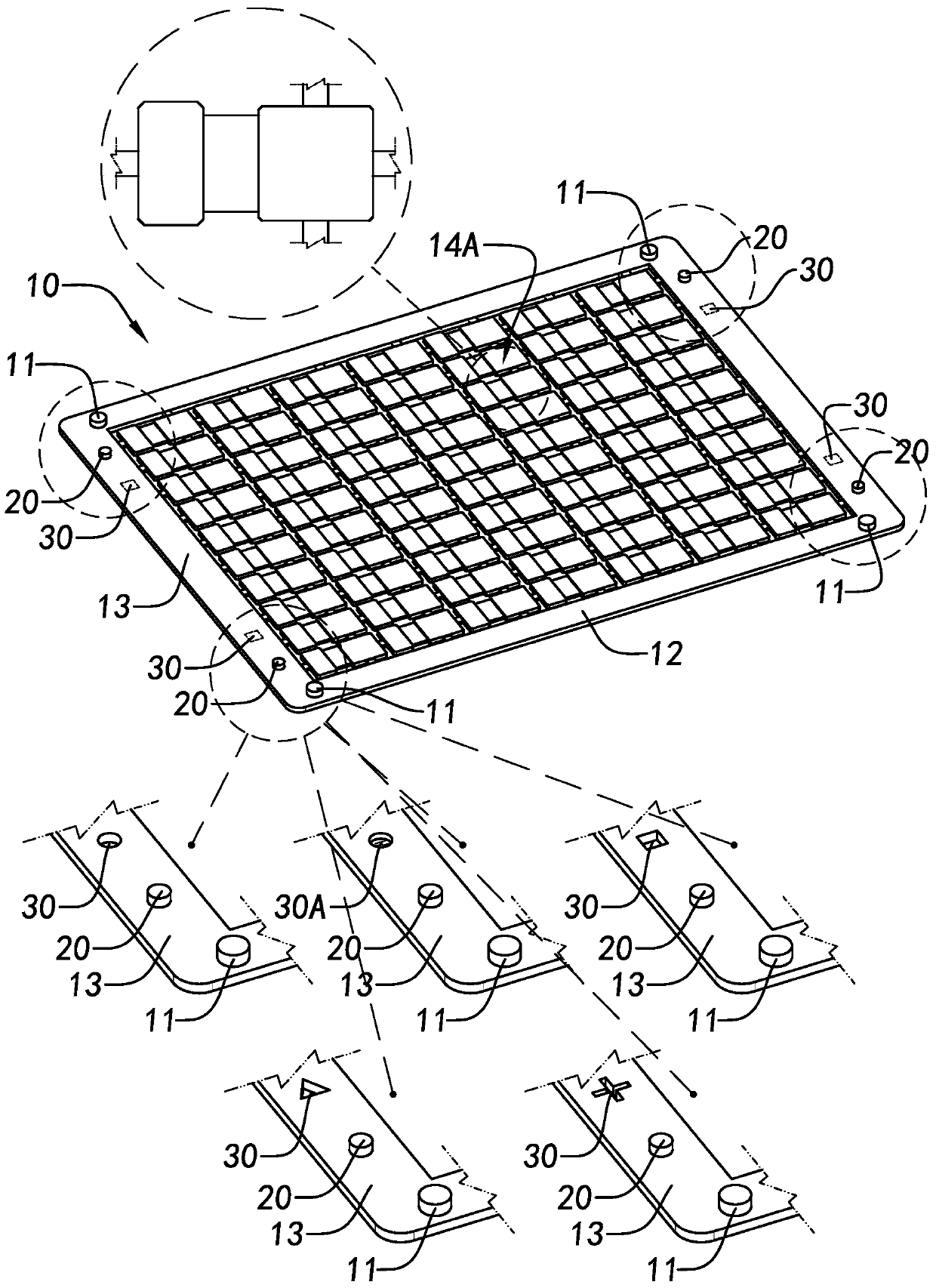
[0037] Such as figure 1 As shown, the four corners of a printed circuit board or printed circuit board (PCB) 10 each have a tool positioning member 11, which can be a positioning post or a positioning hole, and is used for printing circuits and other operations. Positioning, wherein the tool positioning parts are provided on a PCB substrate 12, preferably at four corners, and the PCB substrate can be printed circuit and mounted various co...


PUM


Abstract

The invention discloses a positioning reference point and method for improving cutting precision of a circuit board. The positioning reference points are arranged on a printed circuit board (PCB), the positioning reference points are hollow points and are made by use of the same process as cutting positions of the PCB, each hollow point is completed through primary punching and is arranged at a technical edge of the PCB as a cutting reference point, and thus the laser cutting precision is improved.

Description

Technical field [0001] The present invention relates to the electronics industry that has higher requirements for PCB segmentation and manufacturing, in particular to positioning reference points and methods for improving the cutting accuracy of circuit boards in the mobile phone camera PCB segmentation manufacturing industry, and solves the problem of PCB segmentation by designing positioning coordinates with higher accuracy. Inaccurate positioning coordinates caused by PCB deformation, expansion and contraction, etc. affect the cutting accuracy. Background technique [0002] With the gradual development of electronic products in the direction of fineness, smallness, lightness, and miniaturization, “dimensions” have become one of the important selling points of terminal products. The proposal of high quality and the application of high technology have also brought a lot to the manufacturing process. Series of new challenges. [0003] At present, the SMT process technology used as...

Claims


Application Information

Patent Timeline
Patent Type & Authority Patents(China)
IPC IPC(8): H05K1/02H05K3/00
Inventor 赵丹丹易峰亮李海陈小康舒文良褚斌杰刘海滨
Owner NINGBO SUNNY OPOTECH CO LTD
Why Eureka
Try Eureka