Fingerprint recognition display device

A display device and fingerprint recognition technology, which is applied in character and pattern recognition, acquisition/organization of fingerprints/palmprints, instruments, etc., can solve the problems of mutual interference between fingerprint recognition detection signals and display signals, and affect the quality of fingerprint recognition

Pending Publication Date: 2016-12-14
BOE TECH GRP CO LTD
View PDF6 Cites 76 Cited by
  • Summary
  • Abstract
  • Description
  • Claims
  • Application Information

AI Technical Summary

Problems solved by technology

At present, fingerprint recognition display panels generally adopt capacitive structure to realize the function of fingerprint recognition. For example, in-cell fingerprint recognition display Fingerprint identification components are easy to generate parasitic capacitance with the components inside the display panel, which makes the fingerprint identification detection signal and display signal interfere with each other, thus affecting the quality of fingerprint identification

Method used


Image

  • Fingerprint recognition display device
  • Fingerprint recognition display device
  • Fingerprint recognition display device

Examples


Embodiment Construction

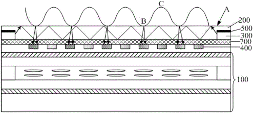
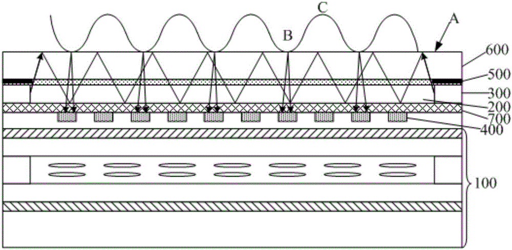
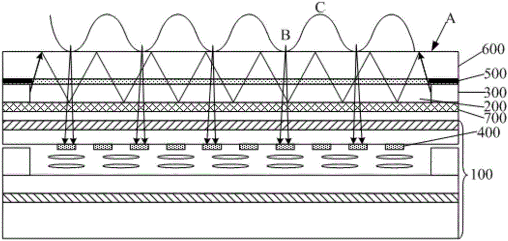
[0022] The specific implementation manner of the fingerprint identification display device provided by the embodiment of the present invention will be described in detail below with reference to the accompanying drawings.

[0023] The shapes and sizes of the components in the drawings do not reflect the true proportions of the fingerprint recognition display device, and the purpose is only to schematically illustrate the content of the present invention.

[0024] An embodiment of the present invention provides a fingerprint identification display device, such as figure 1 As shown, it includes: a display panel 100, a light guide plate 200 disposed on the light-emitting surface of the display panel 100, used to transmit the emitted modulated light between the light guide plate 200 and the display surface A of the display device in a total reflection manner The light emitting component 300 , and a plurality of photosensitive units 400 arranged in an array arranged under the light...


PUM


Abstract

The invention discloses a fingerprint recognition display device. The display device comprises a light guide plate, a light emitting component and a plurality of photosensitive induction units, wherein the light guide plate is arranged on an emergent light face of a display panel, the light emitting component is capable of emitting modulating light which is transmitted between the light guide plate and a display face of the display device by adopting a manner of total reflection, and the photosensitive induction units are arranged below the light guide plate and arranged in an array manner. When a user touches the display face of the display device with a finger, the fingerprint ridge position contacts the display face to destroy the total reflection transmission of the modulating light at the position, and the modulating light is reflected to the photosensitive induction units below the modulating light, the fingerprint valley position does not contact the display face and cannot affect the total reflection transmission of the modulating light, and the photosensitive induction units below the modulating light cannot receive the modulating light, thus, the detection on fingerprint can be realized by the photosensitive induction units on the basis of photodynamic action, interference with inner part of the display device is not liable to occur, the influence caused by the distance between the photosensitive induction units and the display face of the display device is not liable to occur, and high-quality fingerprint detection can be easily realized.

Description

technical field [0001] The invention relates to the field of display technology, in particular to a fingerprint identification display device. Background technique [0002] With the rapid development of display technology, display panels with a fingerprint recognition function have gradually spread in people's lives. At present, fingerprint recognition display panels generally adopt capacitive structure to realize the function of fingerprint recognition. For example, in-cell fingerprint recognition display The fingerprint identification component is likely to generate parasitic capacitance with the components inside the display panel, so that the fingerprint identification detection signal and the display signal interfere with each other, thereby affecting the quality of fingerprint identification. Contents of the invention [0003] In view of this, an embodiment of the present invention provides a fingerprint identification display device for realizing efficient fingerpr...

Claims


Application Information

Patent Timeline
Patent Type & Authority Applications(China)
IPC IPC(8): G06K9/00G06F3/042
CPCG06F3/0421G06F2203/04109G06V40/1324G06V40/1318G06F18/00G06F3/0412
Inventor 王海生董学吕敬吴俊纬刘英明丁小梁
Owner BOE TECH GRP CO LTD
Why Eureka
Try Eureka