A kind of semiconductor device and its manufacturing method, electronic device
A manufacturing method and technology for electronic devices, which are applied in semiconductor/solid-state device manufacturing, semiconductor devices, circuits, etc., can solve problems such as reducing thermal budget, device reliability breakdown, and forward bias temperature instability, and achieve improved reliability. performance, quality improvement
Active Publication Date: 2019-09-27
SEMICON MFG INT (SHANGHAI) CORP
View PDF6 Cites 0 Cited by
- Summary
- Abstract
- Description
- Claims
- Application Information
AI Technical Summary
Problems solved by technology
With the continuous shrinking of the feature size of semiconductor devices, when implementing the post-high-k dielectric layer metal gate process, it is necessary to sequentially deposit the interface after removing the sacrificial dielectric layer and the sacrificial gate material layer before filling the metal gate material. layer, high-k dielectric layer, capping layer, barrier layer, work function metal layer and wetting layer, the process window of
Method used
View moreImage
Smart ImageViewing Examples


Examples
 PUM
| Property | Measurement | Unit |
|---|---|---|
| Thickness | aaaaa | aaaaa |
| Thickness | aaaaa | aaaaa |
Abstract
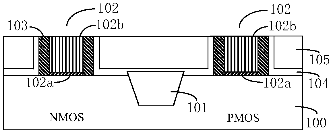
The invention provides a semiconductor device and a manufacturing method thereof and an electronic device. The method comprises the steps that a semiconductor substrate is provided, and pseudo gate structures are formed on the semiconductor substrate; an interlayer dielectric layer is formed on the semiconductor substrate so as to fill the gap between the pseudo gate structures; the pseudo gate structures are removed so that grooves are formed; first preprocessing is performed so as to improve the situation of the side wall and the bottom surface of the grooves; an interface layer is formed on the bottom part of the grooves and second preprocessing is performed so as to improve the surface characteristic of the interface layer; a high-k dielectric layer is formed on the side wall of the grooves and the top part of the interface layer; and a cover layer is formed on the high-k dielectric layer, wherein the step of performing third reprocessing is also included before formation of the cover layer so as to enhance the quality of the high-k dielectric layer, the step of performing fourth preprocessing is also included after formation of the cover layer and oxygen is driven into the high-k dielectric layer so as to reduce the defect of oxygen vacancy. According to the semiconductor device and the manufacturing method thereof and the electronic device, the quality of the formed interface layer and the high-k dielectric layer can be obviously improved so that the reliability of the device can be enhanced.
Description
technical field [0001] The invention relates to a semiconductor manufacturing process, in particular to a semiconductor device, a manufacturing method thereof, and an electronic device. Background technique [0002] In the manufacturing process of next-generation integrated circuits, a high-k-metal gate process is usually used for the fabrication of complementary metal-oxide-semiconductor (CMOS) gates. For CMOS with a smaller numerical process node, the high-k-metal gate process is usually a gate-last process, and its implementation process is a high-k dielectric layer followed by a metal gate and a high-k dielectric layer followed by a There are two types of metal grids. The implementation process of the former includes: forming a dummy gate structure on a semiconductor substrate, and the dummy gate structure is composed of an interface layer, a high-k dielectric layer, a capping layer and a sacrificial gate material stacked from bottom to top. Layer composition; sidewall...
Claims
Login to View More Application Information
Patent Timeline
 IPC IPC(8): H01L21/28H01L21/336H01L27/092
Inventor 赵杰肖莉红
Owner SEMICON MFG INT (SHANGHAI) CORP
Features
- Generate Ideas
- Intellectual Property
- Life Sciences
- Materials
- Tech Scout
- Unparalleled Data Quality
- Higher Quality Content
- 60% Fewer Hallucinations
Learn More Browse by: Latest US Patents, China's latest patents, Technical Efficacy Thesaurus, Application Domain, Technology Topic, Popular Technical Reports.
© 2025 PatSnap. All rights reserved.Legal|Privacy policy|Modern Slavery Act Transparency Statement|Sitemap|About US| Contact US: help@patsnap.com