
Display panel, display device and manufacturing method of display panel

A technology of a display panel and a manufacturing method, which are applied in the directions of identification devices, static indicators, optics, etc., can solve the problems of insufficient support force of spacers, limited pressure resistance, and aggravated indentation, so as to improve the display effect and support function. Strong and lightening effect of indentation

Active Publication Date: 2017-01-04
BOE TECH GRP CO LTD +1
View PDF11 Cites 22 Cited by
  • Summary
  • Abstract
  • Description
  • Claims
  • Application Information

AI Technical Summary

Problems solved by technology

[0003] The spacers used in the prior art have limited pressure resistance, which makes the surface of the display panel prone to indentation and affects the visual display effect
In addition, in the display panel of organic light-emitting diodes, due to the insufficient support of the spacers on both sides of the glass glue, Newton rings appear on the surface of the panel from time to time, which affects the display effect.
Moreover, in the display panel of the organic light-emitting diode, since the cathode material (mainly magnesium and silver) is usually evaporated using a common mask, the cathode material will be stained on the spacer, and when the spacer is in contact with the package cover , when the cathode material on the spacer sticks to the surface of the package cover, it will cause indentation on the display panel, and because of the low light transmittance of the cathode material, it will aggravate the indentation and affect the display effect

Method used


Image

  • Display panel, display device and manufacturing method of display panel
  • Display panel, display device and manufacturing method of display panel
  • Display panel, display device and manufacturing method of display panel

Examples


Embodiment Construction

[0036] Specific embodiments of the present invention will be described in detail below in conjunction with the accompanying drawings. It should be understood that the specific embodiments described here are only used to illustrate and explain the present invention, and are not intended to limit the present invention.

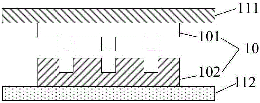
[0037] As a first aspect of the present invention, a display panel is provided, such as figure 1 As shown, it includes a first substrate 111 and a second substrate 112 that are oppositely arranged, and a plurality of spacers 10 are arranged at intervals between the first substrate 111 and the second substrate 112, wherein at least one spacer 10 includes a first support portion 101 and the second support part 102, the first support part 101 is arranged on the first substrate 111, the second support part 102 is arranged on the second substrate 112, the first support part 101 and the second support part 102 are fixedly connected, and the The elastic modulus of the...


PUM


Abstract

The invention discloses a display panel. The display panel comprises a first substrate and a second substrate which are arranged oppositely. Multiple spacers are arranged between the first substrate and the second substrate at intervals, at least one spacer comprises a first supporting portion and a second supporting portion, the first supporting portion is arranged on the first substrate, the second supporting portion is arranged on the second substrate, the first supporting portion and the second supporting portion are fixedly connected, and the material for manufacturing the first supporting portion is smaller than the material for manufacturing the second supporting portion in elasticity modulus. The invention further discloses a display device and a manufacturing method of the display panel. By the adoption of the display panel, the problem that in the prior art, a supporting force is weak due to the pressure resisting capability of the spacers and the like and accordingly the display panel easily produces indentations is solved.

Description

technical field [0001] The present invention relates to the field of display technology, in particular to a display panel, a display device including the display panel, and a manufacturing method of the display panel. Background technique [0002] In the production of display panels, spacers need to be provided. For example, in order to allow liquid crystals to be injected between the upper and lower substrates of the liquid crystal display panel, spacers need to be provided to provide a space between the upper and lower substrates; in the display panel of organic light emitting diodes , in order to prevent the pixels from being crushed, it is necessary to set spacers between the pixels and between the pixels and the glass glue. [0003] The spacers used in the prior art have limited pressure resistance, which makes indentation easily occur on the surface of the display panel, which affects the visual display effect. In addition, in the display panel of the organic light-em...

Claims


Application Information

Patent Timeline
Patent Type & Authority Applications(China)
IPC IPC(8): G02F1/1339G09F9/33
CPCG02F1/13394G09F9/33G02F1/13398G02F1/13396H10K59/8723G09G3/36H10K50/8428H10K59/12H10K59/17H10K71/00H10K85/10
Inventor 王子峰王利娜谷春生白雪飞贾丹
Owner BOE TECH GRP CO LTD
Learn More