Display substrate as well as driving method and display device
A technology for displaying substrates and driving methods, applied to static indicators, instruments, etc., can solve problems such as insufficient charging time, weakened product productivity, and increased charging time, and achieve the goal of avoiding product price increases, avoiding weakened productivity, and increasing charging rates Effect
- Summary
- Abstract
- Description
- Claims
- Application Information
AI Technical Summary
Problems solved by technology
Method used
Image
Examples
Embodiment 1
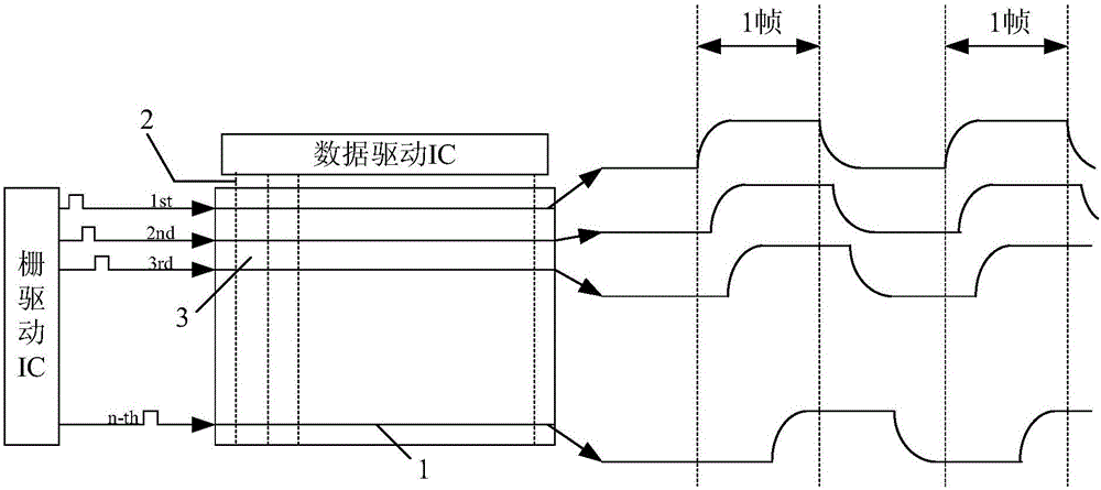
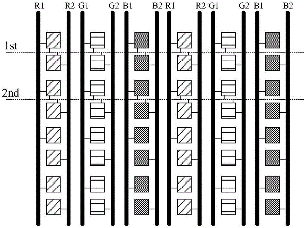
[0032] Please refer to Figure 5 and Image 6 , the present embodiment provides a method for driving a display substrate, the display substrate includes a plurality of data lines and a plurality of gate lines 1, the gate lines and the data lines define a plurality of pixel units, and each pixel unit includes a switching transistor and a switching transistor connected to the pixel electrode. Wherein, the display substrate is connected with the data driving IC and the gate driving IC.
[0033] The driving method of the display substrate in this embodiment includes:
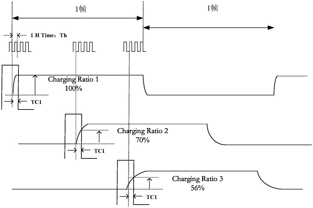
[0034] Step 101 , inputting a gate signal to the gate line, so as to turn on the switch transistor of the pixel unit controlled by the gate line.
[0035] This step is performed by the gate driver IC, that is, the gate driver IC inputs gate signals to the gate lines. That is, the gate drive IC sequentially outputs gate signals to each row of gate lines, so that the gate signals are first input into the pixel uni...
Embodiment 2
[0058] This embodiment provides a display substrate, which is driven by the method for driving the display substrate in Embodiment 1.
[0059] In the display substrate of this embodiment, by controlling the charging time of the image electrode, the charging time of the pixel electrode far away from the signal input end of the data line is longer than the charging time of the pixel electrode close to the signal input end of the data line, so as to increase the signal input far away from the data line The charging rate of the pixel electrode at the end can be avoided, and at the same time, the increase in the number of data lines can be avoided, thereby avoiding the problems of weakening productivity of the product and increasing the price of the product.
Embodiment 3
[0061] This embodiment provides a display panel, including the display substrate of Embodiment 2.
[0062] In the display panel of this embodiment, by controlling the charging time of the image electrode, the charging time of the pixel electrode far away from the signal input end of the data line is longer than the charging time of the pixel electrode close to the signal input end of the data line, so as to increase the signal input far away from the data line The charging rate of the pixel electrode at the end can be avoided, and at the same time, the increase in the number of data lines can be avoided, thereby avoiding the problems of weakening productivity of the product and increasing the price of the product.
PUM
 Abstract
Description
Claims
Application Information


