Wafer transmission device

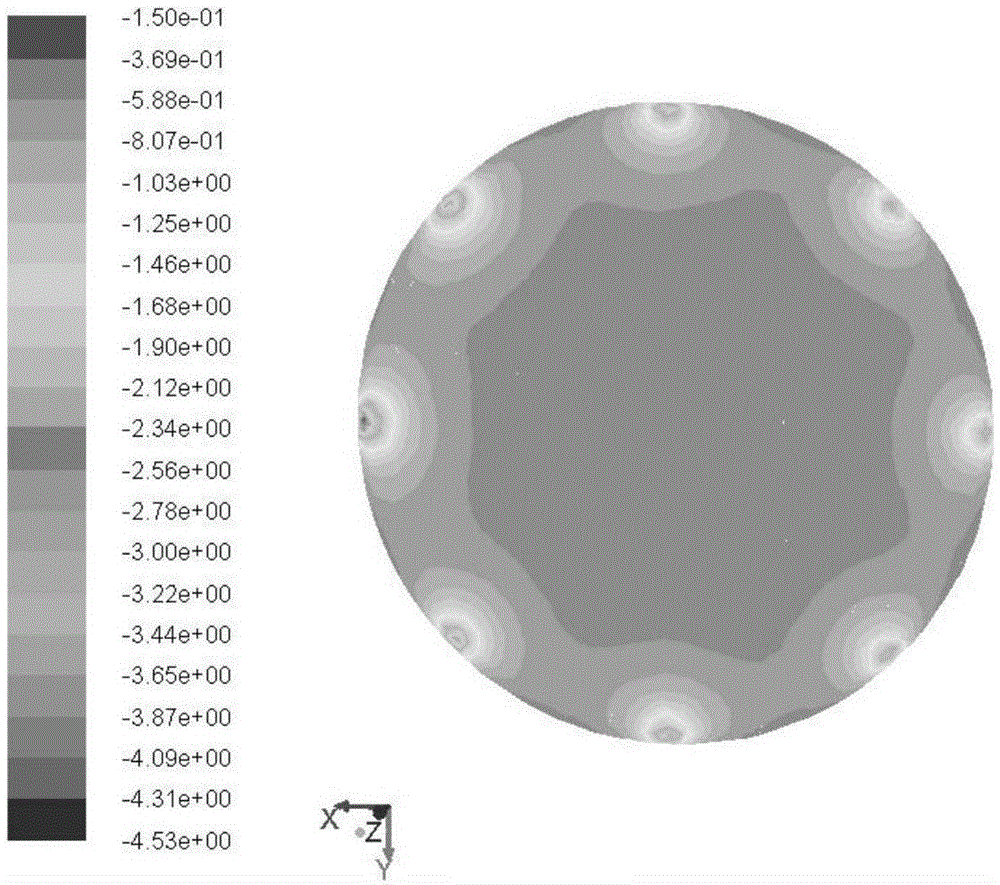
A transmission device and chip technology, applied in the direction of transportation and packaging, conveyor objects, electrical components, etc., can solve problems such as uneven distribution of adsorption force, shorten the airflow transmission path, improve adsorption force, and improve the uniformity of adsorption force distribution Effect

Inactive Publication Date: 2017-01-04
BEIJING NAURA MICROELECTRONICS EQUIP CO LTD
View PDF5 Cites 4 Cited by
  • Summary
  • Abstract
  • Description
  • Claims
  • Application Information

AI Technical Summary

Problems solved by technology

It can be seen from the figure that the closer the surface of the wafer is to the suction port 15, the more concentrated the adsorption force is, and the greater the adsorption force is, the distribution of the adsorption force on the wafer surface is obviously uneven.

Method used


Image

  • Wafer transmission device
  • Wafer transmission device
  • Wafer transmission device

Examples


Embodiment Construction

[0029] In order to enable those skilled in the art to better understand the technical solution of the present invention, the wafer transfer device provided by the present invention will be described in detail below in conjunction with the accompanying drawings.

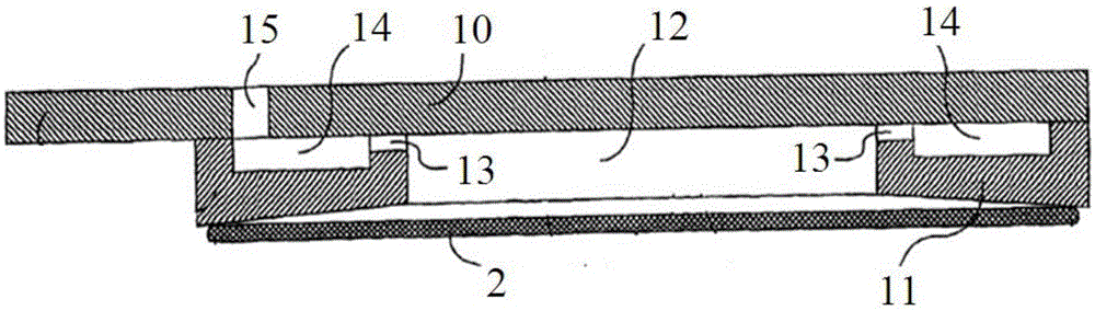
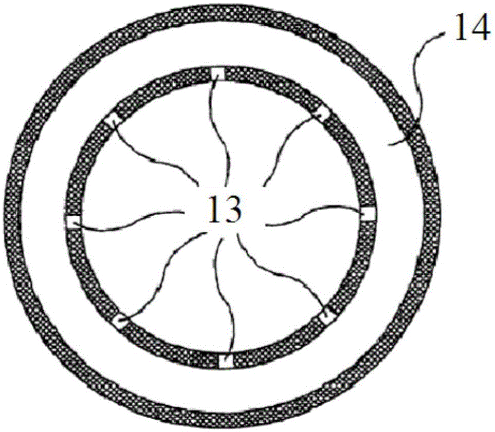
[0030] Please also refer to Figures 4A-4D , the wafer transfer device provided by the embodiment of the present invention includes a plate body, which includes an upper plate 21 and a lower plate 22, wherein the upper plate 21 is a flat plate; grooves are formed on the upper surface of the lower plate 22, and the upper plate 21 and the lower plate 22 When the lower board 22 is docked, the groove and the lower surface of the upper board 21 form an air pumping cavity 23 .

[0031] Moreover, the lower surface of the lower plate 22 is a concave surface 221 , which is used for absorbing the wafer and is only in contact with the edge area of ​​the wafer surface, while the central area of ​​the wafer surface is not in conta...


PUM


Abstract

The invention provides a wafer transmission device, including a plate body in which an exhaust cavity is formed. The plate body comprises a recessed surface for adsorbing a wafer and contacted with the edge area of the surface of the wafer. The recessed surface is provided with multiple exhaust holes communicated with the exhaust cavity. The plate body is also provided with an exhaust opening used for exhausting gas in the exhaust cavity. The wafer transmission device can adsorb the wafer with little negative pressure, so that influences of negative pressure on the cavity pressure are reduced, the adsorption force generated on the surface of the wafer is improved, and the distribution uniformity of the adsorption force is improved.

Description

technical field [0001] The invention relates to the field of semiconductor manufacturing, in particular to a wafer transfer device. Background technique [0002] In the field of semiconductor integrated circuit manufacturing, wafer transfer is very important. The wafer is generally circular and has a front and a back. The front of the wafer is the wafer surface used to realize the integrated circuit structure. Therefore, it is very important to protect the front of the wafer from damage during the wafer transfer process. For this reason, the wafer is generally selected Backside transfer of wafers. However, in some fields of epitaxial reaction, it is not possible to use the back of the wafer to transfer the wafer. In this case, since the edge area of ​​the front of the wafer near its edge is a few millimeters away from the integrated circuit structure, the edge of the front of the wafer can be used by vacuum adsorption. Area transfer wafers. [0003] figure 1 It is a sect...

Claims


Application Information

Patent Timeline
Patent Type & Authority Applications(China)
IPC IPC(8): H01L21/683H01L21/677
CPCH01L21/6838H01L21/677H01L2221/683
Inventor 李伟
Owner BEIJING NAURA MICROELECTRONICS EQUIP CO LTD
Why Eureka
Try Eureka