Stereo electronic packaging structure containing conduction support base material

A technology of electronic packaging and conductive support, which is applied in the direction of semiconductor devices, semiconductor/solid-state device components, circuits, etc., and can solve the problems that heat energy is not easy to be removed, and it is not stackable.

Inactive Publication Date: 2009-07-01
ADVANCED CHIP ENG TECH
View PDF1 Cites 5 Cited by
  • Summary
  • Abstract
  • Description
  • Claims
  • Application Information

AI Technical Summary

Problems solved by technology

The signal transmission of the electronic components in this invention can be connected to the patterned metal layer on the surface of the packaging structure by using the aforementioned conductive via hole. At the same time, the patterned metal layer also provides the function of supporting the packaging structure during the manufacturing process. ; However, this packaging structure does not have the characteristics of being stackable. At the same time, there is a dielectric material barrier between the electronic component and the metal layer except for the via hole. The heat generated by the electronic component is not easy to be discharged to the outside of the package through this way.

Method used


Image

  • Stereo electronic packaging structure containing conduction support base material
  • Stereo electronic packaging structure containing conduction support base material
  • Stereo electronic packaging structure containing conduction support base material

Examples


Embodiment Construction

[0072] The aforesaid and other objects, features and advantages of the present invention will be made clearer through the following detailed description with reference to the illustrated preferred embodiments.

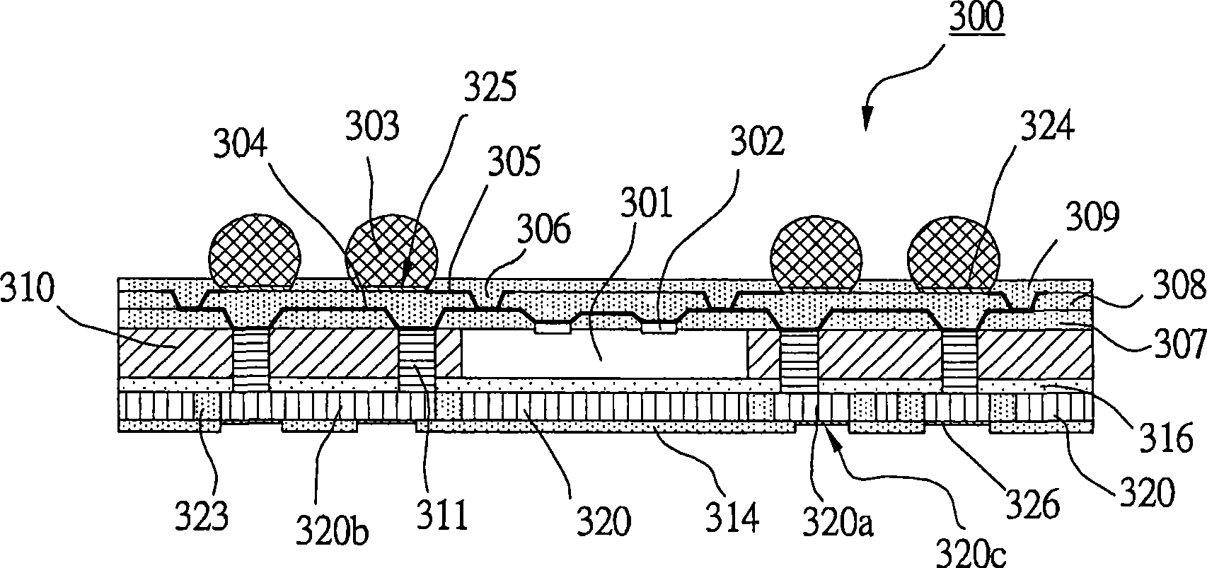
[0073] The invention discloses an electronic packaging structure. More specifically, the present invention provides a packaging unit with a conductive support base plate. The packaging unit can achieve the purpose of multi-chip stacking through the telecommunication contacts on both sides. The embodiments of the invention are described in detail as follows, but the preferred embodiments described are only for illustration and are not intended to limit the invention.

[0074] Figure 3a It is a cross-sectional view of the packaging unit of the present invention. The first packaging unit body 300 uses a supporting base plate 320 as a structural skeleton. The supporting base plate 320 with conductive properties can be copper, nickel, iron, aluminum, cobalt, gold or the a...


PUM


Abstract

The invention provides a stereoscopic electronic packaging structure containing conducting support base plates, which can achieve the purpose of multi-chips to stack through two lateral telecommunication contacts and can be batch-manufactured on wafers or base plates, thereby lowering the manufacturing cost of a single packaging unit body. Supporting bedplates with electrical conductivity are also used for electronic elements to telecommunicate and transfer, the supporting bedplates can also be used as the ground terminals bearing electronic elements, which enhances electrical characteristics of the electronic elements, the supporting bedplates are also thermal good conductors, which can effectively circulate the thermal energy produced and accumulated by the electronic elements in a packaging body to discharge to the outside of the packaging body, thereby increasing the reliability of the packaging body.

Description

technical field [0001] The present invention relates to an electronic packaging structure, in particular to a three-dimensional electronic packaging structure comprising a conductive support base material, in particular to a telecommunication (signal) structure comprising a conductive support base plate which can pass through both sides of the packaging unit The contact is used to achieve the purpose of multi-chip stacking (stracking) packaging unit. Background technique [0002] With the sharp increase in the functions and applications of electronic products, packaging technology continues to develop in the direction of ultra-high density, micro-miniature, single-chip to multi-chip, two-dimensional to three-dimensional, and so on. Advanced packaging structures (such as ultra-high-density packaging forms) are completely different in design, production, and material application, such as wafer-level packaging and three-dimensional packaging; multi-chip packaging and system-in-...

Claims


Application Information

Patent Timeline
Patent Type & Authority Applications(China)
IPC IPC(8): H01L23/488H01L23/492H01L25/00H01L23/36
CPCH01L24/19H01L2224/12105H01L2224/16225H01L2224/19H01L2224/32225H01L2224/73267H01L2225/1035H01L2225/1058H01L2924/15311H01L2924/00012
Inventor 游明志袁长安周展延江国宁
Owner ADVANCED CHIP ENG TECH
Why Eureka
Try Eureka