Fingerprint identification display device, manufacturing method and driving method thereof

A display device and fingerprint recognition technology, which is applied to static indicators, character and pattern recognition, and acquisition/organization of fingerprints/palmprints. question

Active Publication Date: 2017-01-25
BOE TECH GRP CO LTD +1
View PDF5 Cites 51 Cited by
  • Summary
  • Abstract
  • Description
  • Claims
  • Application Information

AI Technical Summary

Problems solved by technology

At present, fingerprint recognition display panels generally adopt capacitive structure to realize the function of fingerprint recognition. For example, in-cell fingerprint recognition display Fingerprint identification components are easy to generate parasitic capacitance with the components inside the display panel, which makes the fingerprint identification detection signal and display signal interfere with each other, thus affecting the quality of fingerprint identification

Method used


Image

  • Fingerprint identification display device, manufacturing method and driving method thereof
  • Fingerprint identification display device, manufacturing method and driving method thereof
  • Fingerprint identification display device, manufacturing method and driving method thereof

Examples


Embodiment Construction

[0037] The specific implementation manners of the fingerprint identification display device provided by the embodiments of the present invention, its manufacturing method and driving method will be described in detail below with reference to the accompanying drawings.

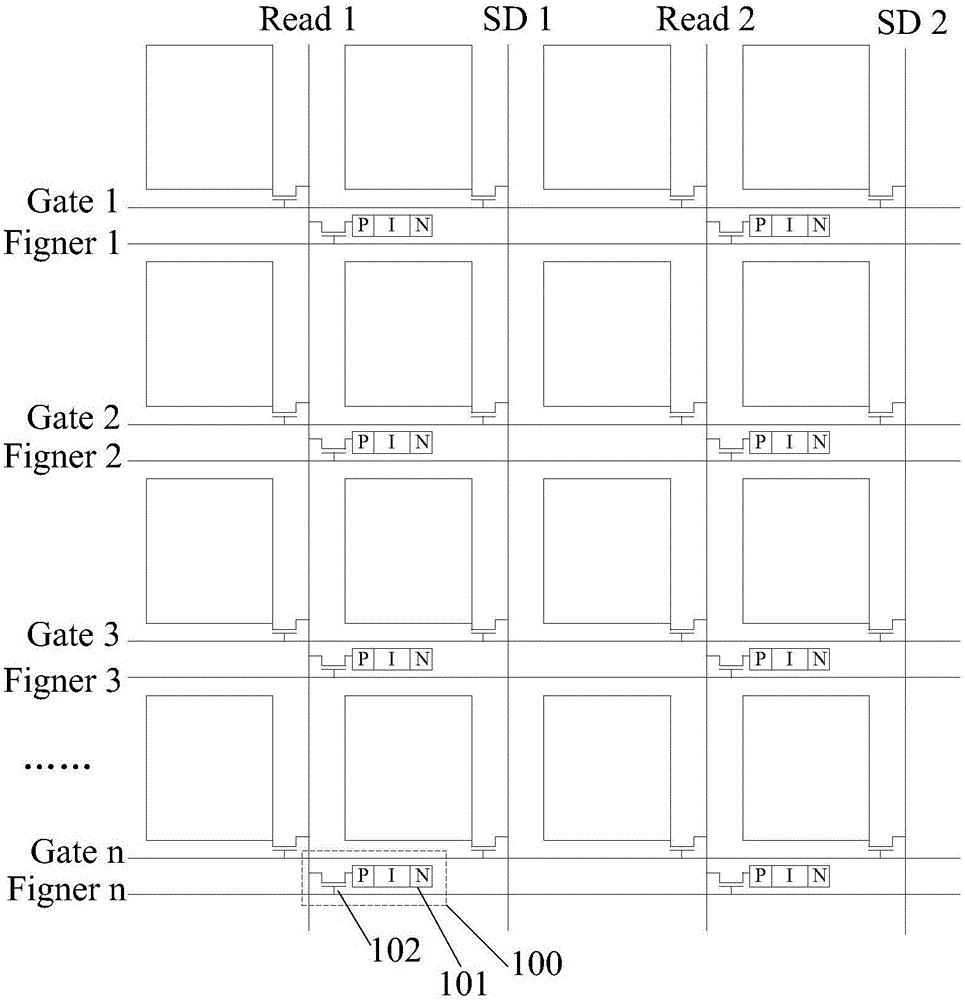
[0038] An embodiment of the present invention provides a fingerprint identification display device, such as figure 1 As shown, it includes: a plurality of photosensitive sensing units 100 arranged in an array arranged inside the display device, a plurality of identification scanning lines Finger 1 to n, and a plurality of identification output lines Read 1 and 2; wherein,

[0039] Each photosensitive unit 100 includes: a photodiode 101 for sensing a change in light intensity when a fingerprint is pressed, and a control switch transistor 102 for controlling the photodiode 101 to convert the light intensity change into a different potential output;

[0040] Each identification scanning line Finger 1 to n is in on...


PUM


Abstract

The invention discloses a fingerprint identification display device, and a manufacturing method and a drive method of the fingerprint identification display device. A plurality of photosensitive sensing units are arranged at the inner part of a display device; every photosensitive sensing unit includes a photosensitive diode used for sensing light intensity change in fingerprint pressing, and a control switch transistor for controlling the photosensitive diode to transform the light intensity change to different potential outputs; the display device further comprises a part for emitting the sensible light of the photosensitive diode. When fingers of a user close to the surface of the device, for the finger skin surface has uneven ridge and valley, the light intensity of irradiating the sensible light of the photosensitive diode sent by the display device to the ridge of the finger is different to the light intensity of the photosensitive diode reflecting valley position to the photosensitive sensing unit. The light intensity difference is transformed to be current signal difference, thus the detection of fingerprint is realized; the photosensitive sensing unit can detect the fingerprint on the basis of the photosensitive effect, and is not easy disturb internal parts of the display device, and easy to realize the high-quality fingerprint detection.

Description

technical field [0001] The invention relates to the field of display technology, in particular to a fingerprint identification display device, a manufacturing method and a driving method thereof. Background technique [0002] With the rapid development of display technology, display panels with a fingerprint recognition function have gradually spread in people's lives. At present, fingerprint recognition display panels generally adopt capacitive structure to realize the function of fingerprint recognition. For example, in-cell fingerprint recognition display The fingerprint identification component is likely to generate parasitic capacitance with the components inside the display panel, so that the fingerprint identification detection signal and the display signal interfere with each other, thereby affecting the quality of fingerprint identification. Contents of the invention [0003] In view of this, the embodiments of the present invention provide a fingerprint identifi...

Claims


Application Information

Patent Timeline
Patent Type & Authority Applications(China)
IPC IPC(8): G06K9/00G09G3/36
CPCG09G3/36G06V40/1318G06V40/1306G06F3/041G09G2310/0278H01L31/02024
Inventor 刘英明董学薛海林陈小川王海生丁小梁杨盛际许睿李昌峰王磊刘伟王鹏鹏
Owner BOE TECH GRP CO LTD
Why Eureka
Try Eureka