Method for improving NMOS hot carrier effect

A hot carrier and effect technology, applied in electrical components, semiconductor/solid-state device manufacturing, circuits, etc., can solve the problems of affecting the lateral electric field of 5V devices, increasing the lateral electric field of 5V devices, etc., to improve the hot carrier effect, The effect of avoiding the influence of the transverse electric field

Active Publication Date: 2017-02-01
SHANGHAI INTEGRATED CIRCUIT RES & DEV CENT +1
View PDF3 Cites 0 Cited by
  • Summary
  • Abstract
  • Description
  • Claims
  • Application Information

AI Technical Summary

Problems solved by technology

Under such constraints, the source-drain injection will affect the lateral electric field of the 5V device, which will increase the lateral electric field of the 5V device due to the high doping of the source and drain

Method used


Image

  • Method for improving NMOS hot carrier effect
  • Method for improving NMOS hot carrier effect
  • Method for improving NMOS hot carrier effect

Examples


Embodiment Construction

[0029] In order to make the content of the present invention clearer and easier to understand, the content of the present invention will be further described below in conjunction with the accompanying drawings. Of course, the present invention is not limited to this specific embodiment, and general replacements known to those skilled in the art are also covered within the protection scope of the present invention.

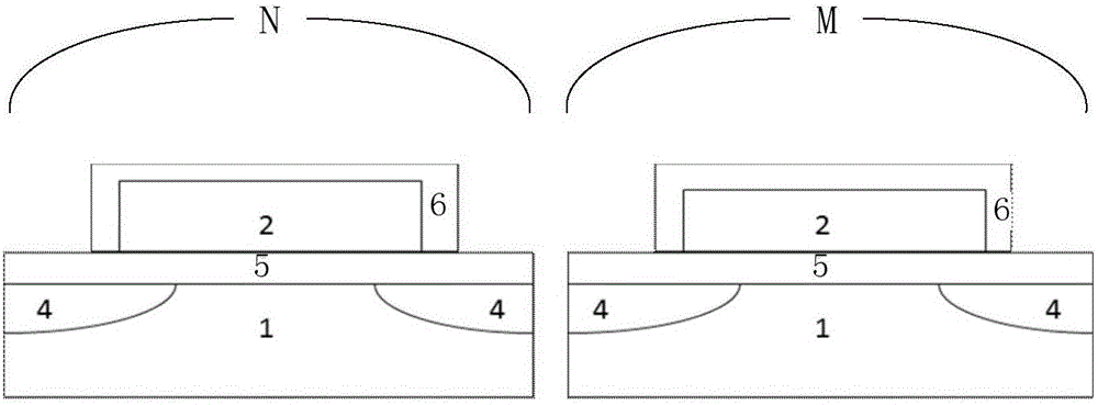
[0030] In the present invention, the first NMOS device region can be applied to a first voltage, the second device region can be applied to a second voltage, and the first voltage is higher than the second voltage. In the present invention, the size of the first sidewall of the first NMOS device region and the second device region may be smaller than or equal to the first size.

[0031] The following is attached Figure 1-12 The present invention will be described in further detail with specific examples. It should be noted that the drawings are all in a very sim...


PUM


Abstract

The invention provides a method for improving an NMOS hot carrier effect. A silicon oxide layer is used as a protection layer for etching a part of silicon nitride layer in a second device region; the residual silicon nitride layer in the second device region is used as a protection layer for etching a silicon oxide layer in a first NMOS device region so as to realize a condition that the silicon nitride layer in the first NMOS device region is thicker than the silicon nitride layer in the second device region; then a silicon nitride material is deposited in the first NMOS device region and the second device region at the same time to increase the thickness of the silicon nitride layer so as to enable the silicon nitride layer in the second device region to achieve the target thickness; therefore, the thickness of a first two-side wall formed in the first NMOS device region through subsequent etching is greater than that of a second two-side wall in the second device region; and due to the different thicknesses of the side walls, the transverse widths of source and drain regions formed in deep well regions at the bottoms on the two sides of the side walls formed in the first NMOS device region and the second device region in subsequent source and drain ionic implantation are different, so that influence to a transverse electric field in the first NMOS device region after the source and drain ionic implantation can be avoided.

Description

technical field [0001] The invention relates to the technical field of integrated circuits, in particular to a method for improving NMOS hot carrier effect. Background technique [0002] As the size of the device shrinks, the influence of the series resistance on the drive current of the device increases. In order to obtain a sufficient drive current, the series resistance needs to be reduced. The LDD of the device contributes more to the series resistance due to its lower doping than the source and drain. Therefore, as the size of the device shrinks, it becomes a trend to reduce the length of the LDD portion, that is, reduce the width of the sidewall. The sidewall width of 5V devices can reach 250nm, but the sidewall width of 60nm devices can reach 60nm or even smaller. [0003] All the devices in the traditional process use the same width of the spacer. Under such constraints, the source-drain injection will affect the lateral electric field of the 5V device, and due to...

Claims


Application Information

Patent Timeline
IPC IPC(8): H01L21/336H01L21/28H01L29/10H01L29/423
Inventor 孙德明
Owner SHANGHAI INTEGRATED CIRCUIT RES & DEV CENT
Why Eureka
Try Eureka