A kind of strained channel transistor and its preparation method

A strained channel and transistor technology, which is applied in semiconductor/solid-state device manufacturing, semiconductor devices, electrical components, etc., can solve the problems of reducing device performance, affecting channel carrier mobility, affecting device performance, etc. Carrier mobility, improvement of hot carrier effect, and effect of improving device performance

Active Publication Date: 2018-05-01
SEMICON MFG INT (SHANGHAI) CORP +1
View PDF3 Cites 0 Cited by
  • Summary
  • Abstract
  • Description
  • Claims
  • Application Information

AI Technical Summary

Problems solved by technology

[0005] In order to obtain channel transistors with better performance, SiGe substrates and spacers are generally used in the current HKMG process of 65nm and below, and LDD processes are used to improve junction capacitance and junction leakage current. During the process, it was found that the devices prepared by the above technical scheme had poor NBTI (Negative BiasTemperature Instability, negative bias temperature instability) and HCI (hot-carrier injection, hot carrier effect), while DIBL (Drain Induced Barrier Lowering (drain-induced barrier lowering effect) and Ioff (leakage current) also have a certain gap with expectations, which is due to the higher stress effect of the SiGe channel material layer near the gate edge, which affects the performance of the device
[0006] In the prior art, in order to suppress the above-mentioned adverse effects of the source and drain on the channel, after the channel is formed, the source and drain can be etched away and then the SiC epitaxial layer can be grown, but during this process, the growth on both sides The SiC epitaxial layer will produce compressive stress on the channel, which will also affect the channel carrier mobility, thereby reducing device performance

Method used


Image

  • A kind of strained channel transistor and its preparation method
  • A kind of strained channel transistor and its preparation method
  • A kind of strained channel transistor and its preparation method

Examples


Embodiment Construction

[0052] The specific embodiment of the present invention will be further described below in conjunction with accompanying drawing:

[0053] like Figures 1 to 8 As shown, a preparation method of a strained channel transistor in the present application includes the following steps:

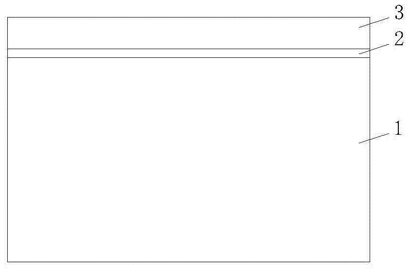
[0054] Step S1: Provide an SOI (Silicon On Insulator, silicon on insulator) structure, which includes a substrate 1, a buried oxide layer 2, and a silicide layer 3 from bottom to top; preferably, the substrate 1 is germanium (Ge) The substrate, the material of the silicide layer 3 is silicon nitride (SiC), and the thickness of the silicide layer 3 is 20-50 nm, such as figure 1 structure shown. In the embodiment of the present invention, whether to pre-dope the source and drain of the silicide layer 3 is selected according to the process requirements, and specific related descriptions can be found below;

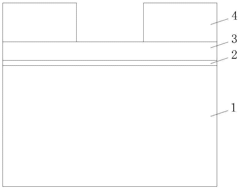
[0055] Deposit a mask layer 4 to cover the upper surface of the silicide layer 3, perform a ...


PUM


Abstract

The invention provides a strain channel transistor and a manufacturing method thereof. Firstly, a SOI (Silicon On Insulator) structure is provided; then, a mask layer is deposited above the SOI structure, etching is carried out until the substrate of the SOI structure, and a channel is formed; then, epitaxial growth of a layer of Ge material layer and a Si material layer is carried out in the channel to define a channel region, and side wall manufacturing and gate manufacturing are completed above the channel; and finally, the mask layer is removed, an epitaxial layer grows on a source / drain again and a doped manufacturing process for the source / drain is carried out. As Si has a smaller lattice constant than Ge, the Ge material layer generates a high strain in the channel, carrier mobility of the channel is improved, hot-carrier injection can be significantly improved, and device performance is enhanced.

Description

technical field [0001] The invention relates to the field of semiconductor preparation, in particular to a strained channel transistor and a preparation method thereof. Background technique [0002] In the prior art, in order to meet the trend of low power and high operating efficiency of transistors, strained channel transistors have been developed, the channels of which are formed with large lattice parameters, thereby increasing the mobility of charges through the channel. [0003] With people's continuous pursuit of high-performance semiconductor devices, the critical dimensions of MOSFETs continue to shrink, and the reduction of critical dimensions means that more transistors can be arranged on and off the chip, thereby improving device performance. However, as the device area continues to shrink, problems also follow. Due to the limitations of existing processes and equipment, it is difficult to prepare a completely ideal gate oxide layer, and the power supply voltage ...

Claims


Application Information

Patent Timeline
Patent Type & Authority Patents(China)
IPC IPC(8): H01L21/336H01L21/28H01L29/78H01L29/10H01L29/40
CPCH01L29/0603H01L29/1033H01L29/1054H01L29/42312H01L29/66477H01L29/7849
Inventor 赵猛
Owner SEMICON MFG INT (SHANGHAI) CORP
Why Eureka
Try Eureka