
A kind of radio frequency ldmos device and its manufacturing method

A manufacturing method and device technology, applied in semiconductor/solid-state device manufacturing, semiconductor devices, electrical components, etc., can solve problems such as high doping concentration, hot carrier injection effect, etc., to reduce channel resistance and improve reliability performance, improving the effect of hot carrier effect

Active Publication Date: 2016-02-10
SHANGHAI HUAHONG GRACE SEMICON MFG CORP
View PDF4 Cites 0 Cited by
  • Summary
  • Abstract
  • Description
  • Claims
  • Application Information

AI Technical Summary

Problems solved by technology

The main reason is that when a high voltage is applied to the drain terminal 9, the lateral electric field of the drift region 3 is stronger; the doping concentration of the drift region 3 under the polysilicon gate 5 is higher, so the lateral electric field is stronger, thereby causing severe heat-carrying current sub-injection effect

Method used


Image

  • A kind of radio frequency ldmos device and its manufacturing method
  • A kind of radio frequency ldmos device and its manufacturing method
  • A kind of radio frequency ldmos device and its manufacturing method

Examples


Embodiment Construction

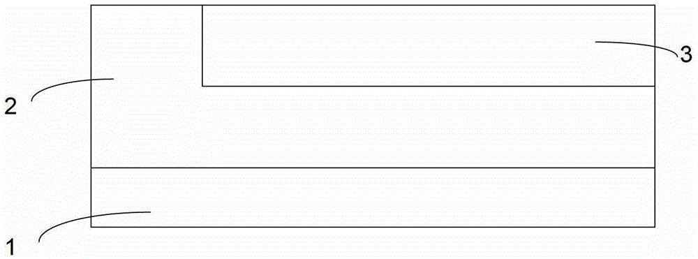
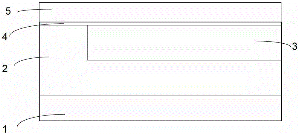
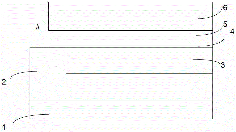
[0017] See Figure 1i , This is the radio frequency LDMOS device described in this application. Taking an n-type radio frequency LDMOS device as an example, a p-type lightly doped epitaxial layer 2 is provided on a p-type heavily doped substrate 1. The epitaxial layer 2 has an n-type heavily doped source region 8, a p-type channel doped region 7 and an n-type drift region 3 that are in side contact in sequence. There is an n-type heavily doped drain region 9 in the drift region 3. A gate oxide layer 4 and a polysilicon gate 5 are sequentially arranged on the channel doped region 7 and the drift region 3. The doping concentration of the drift region 3 is not uniform, and the end of the drift region 3 that is in contact with the side surface of the channel doped region 7 (that is, the part of the drift region 3 under the gate oxide layer 4) has a lower doping concentration than the rest Part of the doping concentration of the drift region 3. A piece of silicon oxide 10 is conti...


PUM


Abstract

The invention discloses a radio frequency LDMOS (laterally diffused metal oxide semiconductor) device. The side surface of a channel doping region and the side surface of a drift region of the radio frequency LDMOS device are contacted; a gate oxide and a grid electrode are successively arranged above the channel doping region and the drift region; and the doping density of the part of the drift region, which is below the channel doping region, is smaller than the doping density of rest parts. The invention also discloses a manufacture method for the radio frequency LDMOS device. Because the doping density of the drift region is unevenly distributed, the hot carrier effect can be lowered while the low-conduction resistance is obtained.

Description

Technical field [0001] This application relates to a semiconductor device, in particular to an LDMOS device applied in the radio frequency field. Background technique [0002] Radio frequency LDMOS (laterally diffused MOS transistor) devices are commonly used devices in radio frequency base stations and broadcasting stations. The performance indicators they pursue include high breakdown voltage, low on-resistance, and low parasitic capacitance. [0003] See Figure 1i , This is an existing RF LDMOS device. Taking an n-type radio frequency LDMOS device as an example, a p-type lightly doped epitaxial layer 2 is provided on a p-type heavily doped substrate 1. The epitaxial layer 2 has an n-type heavily doped source region 8, a p-type channel doped region 7 and an n-type drift region 3 that are in side contact in sequence. The doping concentration of the drift region 3 is uniform. The drift region 3 has an n-type heavily doped drain region 7. A gate oxide layer 4 and a polysilicon g...

Claims


Application Information

Patent Timeline
Patent Type & Authority Patents(China)
IPC IPC(8): H01L29/78H01L29/10H01L29/06H01L21/336
Inventor 钱文生
Owner SHANGHAI HUAHONG GRACE SEMICON MFG CORP
Learn More