Insulated gate bipolar transistor

A bipolar transistor, insulated gate technology, applied in semiconductor devices, electrical components, circuits, etc., can solve problems such as weak anti-latch ability, achieve strong conductance modulation effect, ensure device parameter performance, and improve anti-latch ability. Effect

Active Publication Date: 2017-02-15
INST OF MICROELECTRONICS CHINESE ACAD OF SCI
View PDF2 Cites 2 Cited by
  • Summary
  • Abstract
  • Description
  • Claims
  • Application Information

AI Technical Summary

Problems solved by technology

[0007] The present invention solves the technical problem of weak latch-up resistance existing in the PNM-IGBT device in the prior art by providing an insulated gate bipolar transistor

Method used


Image

  • Insulated gate bipolar transistor
  • Insulated gate bipolar transistor

Examples


Embodiment Construction

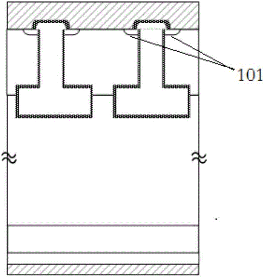
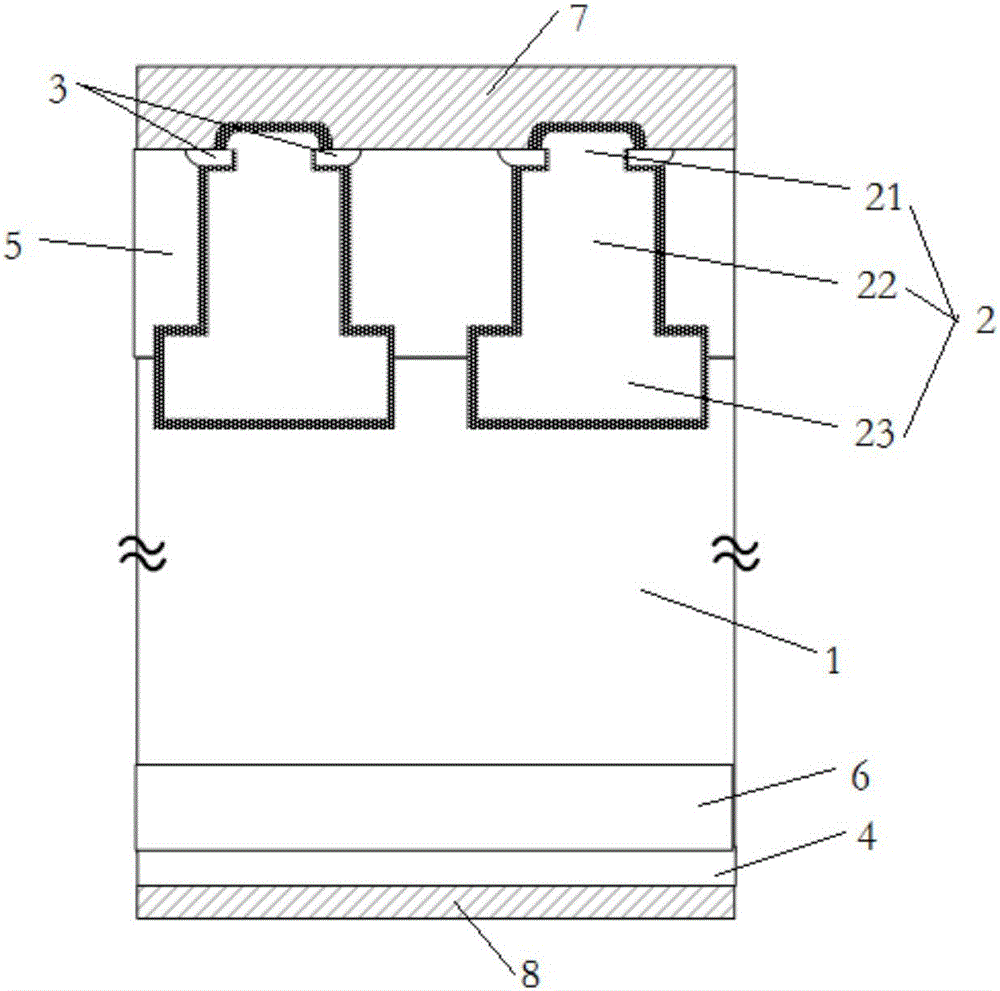
[0027] The embodiment of the present application solves the technical problem of weak latch-up resistance existing in the PNM-IGBT device in the prior art by providing an insulated gate bipolar transistor. The technical effect of significantly improving the anti-latch-up ability is achieved on the basis of ensuring the parameter performance of the device.

[0028] In order to solve the above technical problems, the general idea of ​​the technical solution provided by the embodiment of the present application is as follows:

[0029] The present application provides an insulated gate bipolar transistor, including:

[0030] Substrate;

[0031] A gate structure, an emitter, and a collector located on the substrate; wherein, the collector and the emitter are respectively located at both ends of the substrate; the gate structure includes a narrow portion, a first widening portion and a second widened portion, the narrowed portion is located between the two emitters, the second wid...


PUM


Abstract

The invention discloses an insulated gate bipolar transistor comprising a substrate, gate structures, emitters and a collector. The gate structures, the emitters and the collector are arranged at the substrate; and the collector and the emitters are arranged at the two ends of the substrate. Each gate structure consists of a narrow part, a first widening part, and a second widening part; the narrow part is arranged between two emitters; the second widening part is arranged at one side, approaching the collector, of the gate structure; and the first widening part is connected between the narrow part and the second widening part. The first widening part is wider than the narrow part and thus areas that are connected with the emitter and are arranged in first directions of the emitters are filled, thereby suppressing starting of parasitic transistors at the edges of the emitters; and the second widening part is wider than the first widening part. Therefore, a technical problem of weak anti-latching capability of the existing PNM-IGBT device in the prior art can be solved; and thus a technical effect that the anti-latching capability is improved obviously while the parameter performance of the device is guaranteed is realized.

Description

technical field [0001] The invention relates to the field of semiconductors, in particular to an insulated gate bipolar transistor. Background technique [0002] Insulated Gate Bipolar Transistor (IGBT) is widely used in various power electronic systems due to its low on-state voltage drop, high withstand voltage, simple drive control, and easy parallel connection. One of the core devices. In order to achieve the best performance of the device, it is necessary to realize the parameters of the device as close to the design limit as possible. In the actual device design, due to the mutual restriction of the characteristics of each parameter, the principle of compromise must be followed to select the relative optimal value. It is often difficult to optimize one parameter at the same time as other parameters are also optimized. This poses a great challenge to the design structure. [0003] Sumitomo et al. proposed a structure that uses a partially narrowed gate structure to e...

Claims


Application Information

Patent Timeline
Patent Type & Authority Applications(China)
IPC IPC(8): H01L29/10H01L29/739
CPCH01L29/1066H01L29/7393
Inventor 陆江
Owner INST OF MICROELECTRONICS CHINESE ACAD OF SCI
Why Eureka
Try Eureka