U-type source slot VDMOSFET device with Schottky diode

A Schottky diode, U-shaped technology, applied in the field of microelectronics, can solve the problems of increasing on-resistance and diode forward voltage drop, increasing circuit design complexity and cost, and power-on deterioration.

Active Publication Date: 2019-01-11
XIDIAN UNIV
View PDF3 Cites 0 Cited by
  • Summary
  • Abstract
  • Description
  • Claims
  • Application Information

AI Technical Summary

Problems solved by technology

At the same time, VDMOSFET is used as a power switch in the converter. When its body diode continues to flow forward current as a freewheeling path, the phenomenon of "power-on deterioration" will occur, which will increase the on-resistance and the forward conduction voltage drop of the diode. and cause reliability issues
Therefore, in practical applications, a Schottky diode with a turn-on voltage lower than the body diode is usually connected in parallel at both ends of the source and drain of the device to provide a freewheeling path and ensure that the body diode will not conduct. This method greatly increases reduce the complexity and cost of circuit design

Method used


Image

  • U-type source slot VDMOSFET device with Schottky diode

Examples


Embodiment Construction

[0030] In the following description, many technical details are proposed in order to enable readers to better understand the application. However, those skilled in the art can understand that the technical solutions claimed in this application can be realized even without these technical details and various changes and modifications based on the following implementation modes.

[0031] Explanation of terms involved in this application:

[0032] VDMOSFET, (vertical double-diffused MOSFET): vertical double-diffused metal oxide semiconductor field effect transistor.

[0033] In order to make the object, technical solution and advantages of the present invention clearer, the present invention will be described in further detail below in conjunction with specific examples, but the implementation of the present invention is not limited thereto.

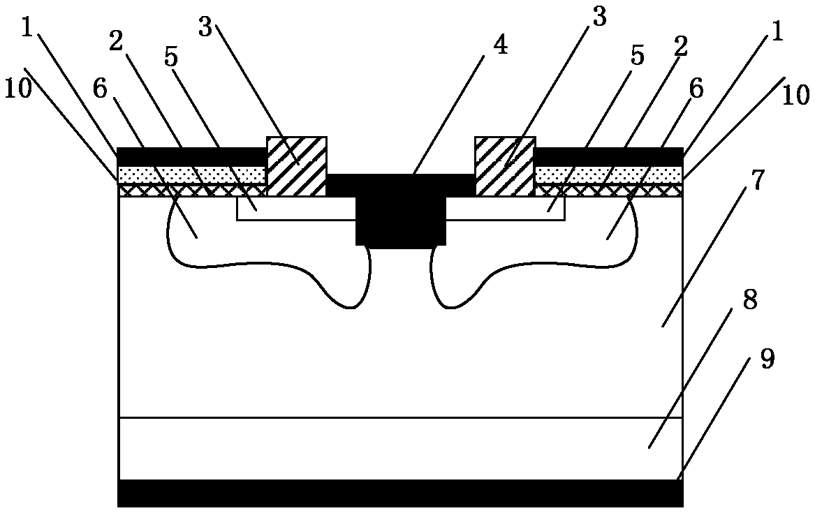
[0034] The first embodiment of the present application relates to a U-shaped source-trough VDMOSFET device integrating a Schottky diode. ...


PUM

PropertyMeasurementUnit
Doping concentrationaaaaaaaaaa
Thicknessaaaaaaaaaa

Abstract

The invention relates to the field of integrated circuits and discloses a U-shaped source slot VDMOSFET device integrated with a Schottky diode, which is characterized in that the device comprises a substrate (8); a drain electrode (9) arranged below the substrate (8); N-drift region (7) arranged above the substrate (8); a source (4) arranged above the N-drift region (7); an N+ source region (5) arranged in the N-drift region on both sides of the source electrode (4); a P-type base region (6) provided in the N-drift region (7); a gate-source isolation layer (3) arranged above the N+ source region (5); a gate dielectric (2) and a gate electrode (10). The interfaces of the source (4) and the N-drift region (7) are in a Schottky contact. The device can improve the reliability of the device performance and reduce the complexity and cost of the design.

Description

technical field [0001] The invention relates to the technical field of microelectronics, in particular to a U-shaped source-trough VDMOSFET device integrating Schottky diodes. Background technique [0002] Silicon carbide, a wide bandgap semiconductor material, has a large band gap, a high critical breakdown electric field, and excellent physical and chemical properties such as high thermal conductivity and high electron saturation drift velocity. It is suitable for making high temperature, high pressure, high power, radiation resistant illuminated semiconductor devices. In the field of power electronics, power MOSFET has been widely used, it has the characteristics of simple gate drive and short switching time. [0003] In the existing VDMOSFET structure, in order to avoid turning on the parasitic NPN transistor, the P-type base region and the N+ source region are usually short-circuited by introducing a P+ ohmic contact region on the surface of the P-type base region. At...

Claims


Application Information

Patent Timeline
IPC IPC(8): H01L29/78H01L29/08
CPCH01L29/0865H01L29/7802H01L29/7806
Inventor 汤晓燕陈辉张玉明宋庆文张艺蒙
Owner XIDIAN UNIV
Why Eureka
Try Eureka