A slot gate igbt device with carrier storage layer

A carrier storage and trench gate technology, applied in semiconductor devices, electrical components, circuits, etc., can solve the problems of limited CSL concentration, small short-circuit safe working area, and high saturation voltage

Active Publication Date: 2020-12-29
杭州朋声科技有限公司
View PDF7 Cites 0 Cited by
  • Summary
  • Abstract
  • Description
  • Claims
  • Application Information

AI Technical Summary

Problems solved by technology

[0004] The object of the present invention is to propose a novel trench gate IGBT with a carrier storage layer for the problems of high saturation voltage, small short-circuit safe working area and limited CSL concentration of the existing trench gate IGBT with a carrier storage layer. IGBT device

Method used


Image

  • A slot gate igbt device with carrier storage layer
  • A slot gate igbt device with carrier storage layer
  • A slot gate igbt device with carrier storage layer

Examples


Embodiment 1

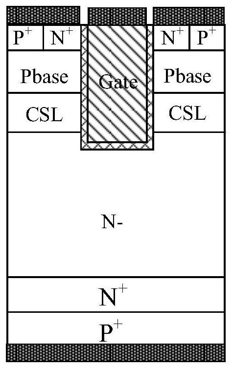
[0026] This embodiment provides a trench gate IGBT device with a carrier storage layer, the cell structure of which is as follows image 3 shown, including:

[0027] The voltage-resistant region 1, the N-type buffer layer 2 disposed at the bottom of the voltage-resistant region 1, the P-type collector semiconductor region 3 disposed on the lower surface of the N-type buffer layer 2, and the P-type collector semiconductor region 3 disposed on the lower surface collector metal 13;

[0028] The P-type electric field shielding layer 11 arranged on the upper surface of the withstand voltage region 1, the N-type carrier storage layer 4 covering the upper surface of the withstand voltage region 1 and the P-type electric field shielding layer 11, and the N-type carrier layer 4 covering the upper surface of the N-type electric field shielding layer 11. P-type base region 5 on the upper surface of sub-storage layer 4;

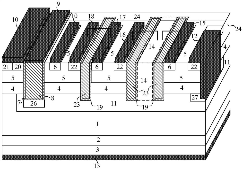
[0029] The surface of the cell is provided with a first deep groo...

Embodiment 2

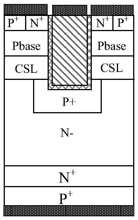
[0038] This embodiment provides a slot gate IGBT device with a carrier storage layer, such as Figure 4 Shown, the difference of its cellular structure and embodiment 1 is:

[0039] The metal short-circuit mode is: the P-type electric field shielding layer 11 is connected to the semiconductor surface through a deeply diffused P-type semiconductor region 25; the deeply diffused P-type semiconductor region 25, the deeply diffused N-type semiconductor region 24 and the second The surface of the nth P-type heavily doped semiconductor region 22 in n PN junction diodes is covered with metal 12; The heavily doped region 6 forms an ohmic contact. The deep diffused P-type semiconductor region 25 can be in direct contact with the metal 12, or can also form an ohmic contact through an n+1th P-type heavily doped semiconductor region 22, and this embodiment provides the situation of direct contact; Its principle and effect are similar with embodiment 1;


PUM


Abstract

The invention relates to the field of power semiconductors, and provides a slot-gate IGBT device with a carrier storage layer (CSL), which is used to solve the problem of high saturation voltage and short-circuit safe working area of ​​the existing slot-gate IGBT with a carrier storage layer (CSL). In view of the problems of small size and limited concentration of CSL, a new trench-gate IGBT device with carrier storage layer is proposed. The IGBT of the present invention directly integrates a plurality of series diodes on the surface of the silicon chip in the trench gate IGBT process to clamp the potential of the electric field shielding layer in the P region, thereby breaking through the concentration limit of CSL on the basis of the existing trench gate IGBT process, and extremely The injection efficiency of the emitter of the IGBT is greatly improved, thereby greatly improving the trade-off relationship between the turn-on voltage drop and the turn-off loss of the IGBT; at the same time, due to the clamping effect of the diode, the drain near the nMOS channel of the IGBT is in the Under high voltage and high current, it is clamped at a lower voltage, so that the saturation current of the new IGBT is greatly reduced, thereby improving the short-circuit safe working area of ​​the IGBT.

Description

technical field [0001] The invention relates to the field of power semiconductors, and provides a slot-gate IGBT device with a carrier storage layer, specifically an IGBT with ultra-low conduction voltage drop, low saturation current density, high safe working area and fast turn-off characteristics device. Background technique [0002] IGBT compromises the low turn-on voltage drop of BJT and the fast switching characteristics of MOSFET, so it is widely used in power electronic systems. [0003] The most critical characteristic of IGBT is the trade-off relationship between turn-on voltage drop and turn-off loss, as well as the safe operating area. When the IGBT is turned on, the collector injects a large number of unbalanced carriers to form a conductance modulation effect to reduce the turn-on voltage drop. When it is turned off, it takes a while for the minority carriers in the withstand voltage region to disappear, which makes the IGBT turn off slower and turn off the los...

Claims


Application Information

Patent Timeline
Patent Type & Authority Patents(China)
IPC IPC(8): H01L29/40H01L29/423H01L29/739
CPCH01L29/401H01L29/42312H01L29/7397H01L29/7398
Inventor 易波李平
Owner 杭州朋声科技有限公司
Why Eureka
Try Eureka