Isolated ldmos structure and manufacturing method thereof

An isolation type and isolation groove technology, which is applied in semiconductor/solid-state device manufacturing, semiconductor devices, electrical components, etc., can solve the contradiction between device withstand voltage and on-resistance, and can not completely improve the problem of device electric field distribution, etc., to achieve process implementation Reduced difficulty, excellent uniformity of concentration distribution, optimized breakdown voltage and specific on-resistance

Active Publication Date: 2019-08-23
UNIV OF ELECTRONICS SCI & TECH OF CHINA
View PDF4 Cites 0 Cited by
  • Summary
  • Abstract
  • Description
  • Claims
  • Application Information

AI Technical Summary

Problems solved by technology

However, this type of structure cannot completely improve the electric field distribution in the device body, and there is still a contradiction between the device withstand voltage and on-resistance

Method used


Image

  • Isolated ldmos structure and manufacturing method thereof
  • Isolated ldmos structure and manufacturing method thereof
  • Isolated ldmos structure and manufacturing method thereof

Examples


Embodiment Construction

[0035] Embodiments of the present invention are described below through specific examples, and those skilled in the art can easily understand other advantages and effects of the present invention from the content disclosed in this specification. The present invention can also be implemented or applied through other different specific implementation modes, and various modifications or changes can be made to the details in this specification based on different viewpoints and applications without departing from the spirit of the present invention.

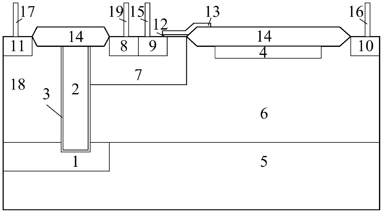
[0036] An isolated LDMOS structure, including an isolation trench structure and an LDMOS structure integrated on the same P-type substrate 5 substrate; the isolation trench structure is located in the P-type substrate 5 and the N-type epitaxial layer 6 above it, Between the second P-type heavily doped region 11 and the first P-type diffused well region 7, the isolation trench structure includes at least one trench 2, a filling medium i...


PUM


Abstract

The invention provides an isolated LDMOS structure and a manufacturing method thereof, comprising an isolation groove structure and an LDMOS structure integrated on the same P-type substrate substrate; the isolation groove structure is located in the P-type substrate and the N-type epitaxial layer above it, Between the second P-type heavily doped region of the LDMOS structure and the first P-type diffused well region, the isolation groove structure includes at least one groove, a filling medium inside the groove, a first P region, and a first oxide layer, and the upper surface of the groove is The third oxide layer of LDMOS; the present invention injects semiconductor impurities of the same doping type as the substrate material in part of the substrate, so that there is a P-type region at the bottom of the formed isolation trench, changing the electric field distribution near the source end, and improving the drift The doping concentration of the region is improved, thereby increasing the device withstand voltage and reducing the specific on-resistance, further optimizing the relationship between the specific on-resistance and the breakdown voltage, and the concentration distribution of the N-type epitaxial layer formed by epitaxy is more uniform.

Description

technical field [0001] The invention belongs to the technical field of semiconductors, and in particular relates to an isolated LDMOS structure and a manufacturing method thereof. Background technique [0002] LDMOS (Lateral Double-Diffused MOSFET) is a commonly used semiconductor device, which has the advantages of high power gain, high efficiency and low cost, and is widely used in semiconductor technology. In order to improve the LDMOS breakdown voltage and increase the output power, the method of increasing the length of the drift region and reducing the doping concentration of the drift region is usually used, which will lead to an increase in the specific on-resistance of the device and increase power consumption. Since the introduction of RESURF technology and slot isolation technology, improved structures such as Single-RESURF LDMOS, Double RESURF LDMOS, Triple RESURF LDMOS, Multiple RESURF LDMOS, 3D RESURFLDMOS, and SJ LDMOS have had a significant effect on reducing...

Claims


Application Information

Patent Timeline
Patent Type & Authority Patents(China)
IPC IPC(8): H01L29/78H01L21/336H01L29/06
CPCH01L29/0611H01L29/0642H01L29/66681H01L29/7816
Inventor 乔明方冬程诗康张波
Owner UNIV OF ELECTRONICS SCI & TECH OF CHINA
Why Eureka
Try Eureka