LDMOS structure in ultrahigh voltage BCD technology

An ultra-high voltage, process technology, applied in the direction of electrical components, circuits, semiconductor devices, etc., to achieve low gate parasitic resistance, increase switching frequency, and reduce parasitic resistance

Inactive Publication Date: 2012-06-13
ADVANCED SEMICON MFG CO LTD
View PDF4 Cites 2 Cited by
  • Summary
  • Abstract
  • Description
  • Claims
  • Application Information

AI Technical Summary

Problems solved by technology

For LDMOS, the essence of its frequency limitation lies in the charging and discharging process of the gate

Method used


Image

  • LDMOS structure in ultrahigh voltage BCD technology
  • LDMOS structure in ultrahigh voltage BCD technology
  • LDMOS structure in ultrahigh voltage BCD technology

Examples


Embodiment Construction

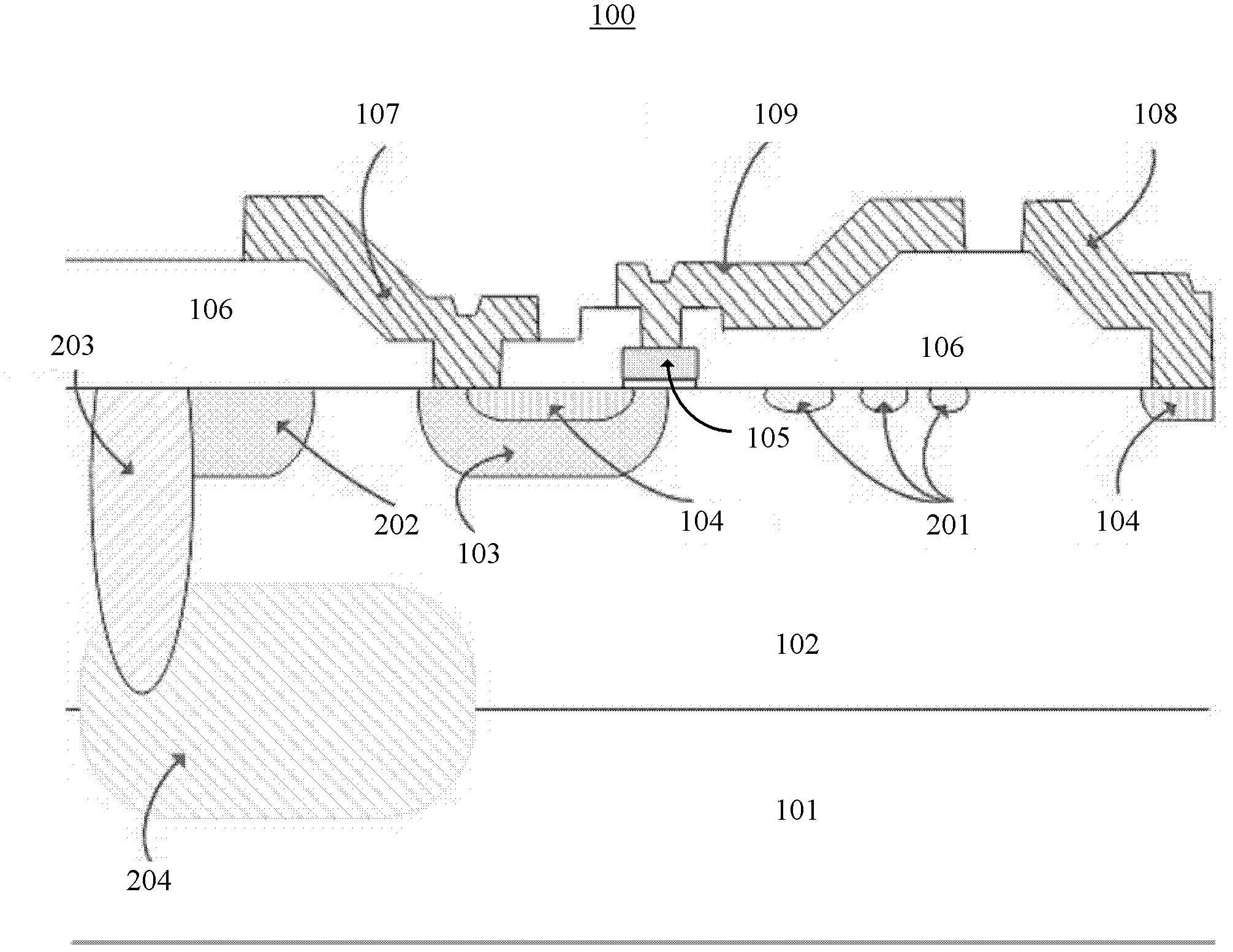
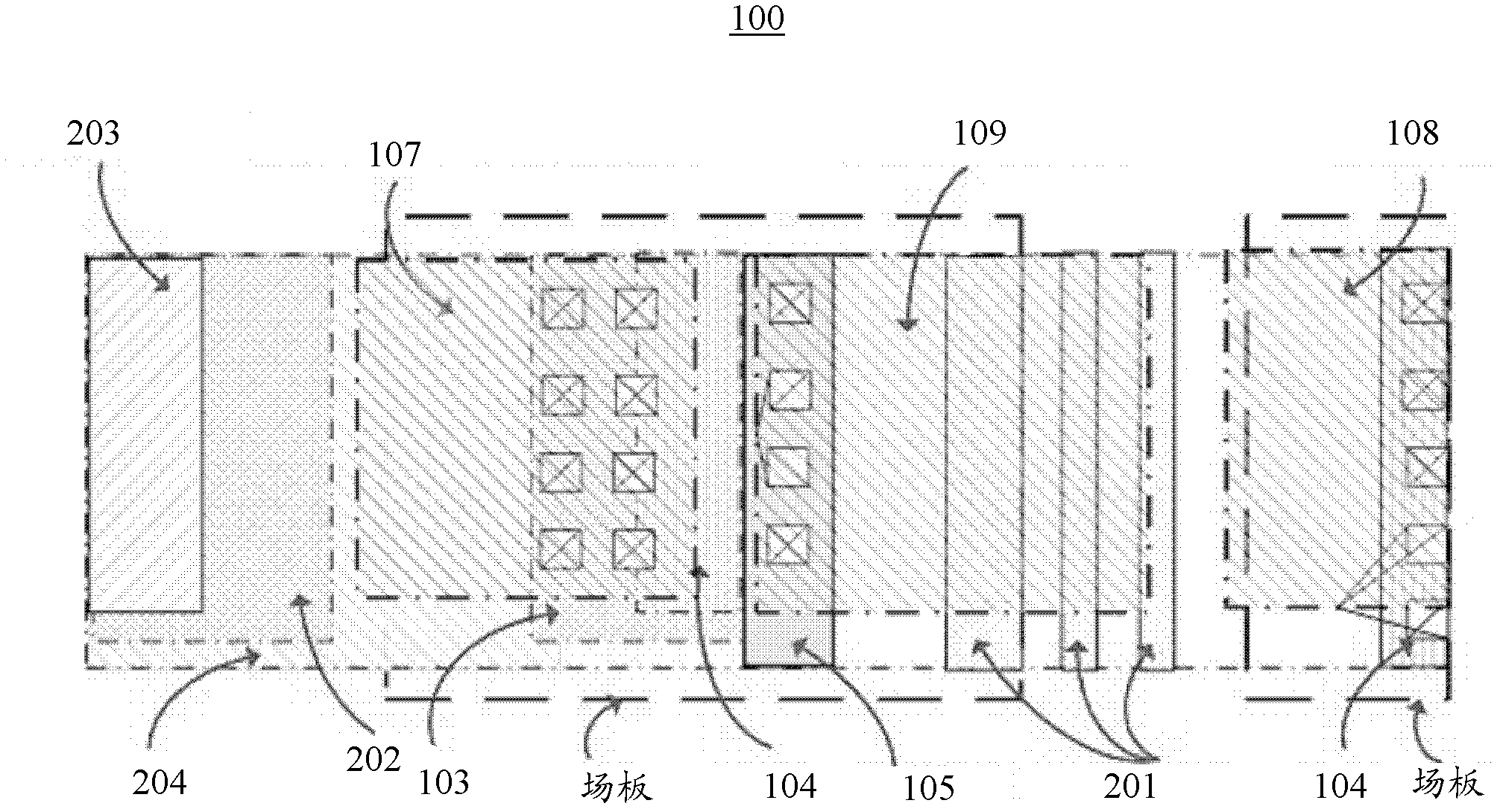
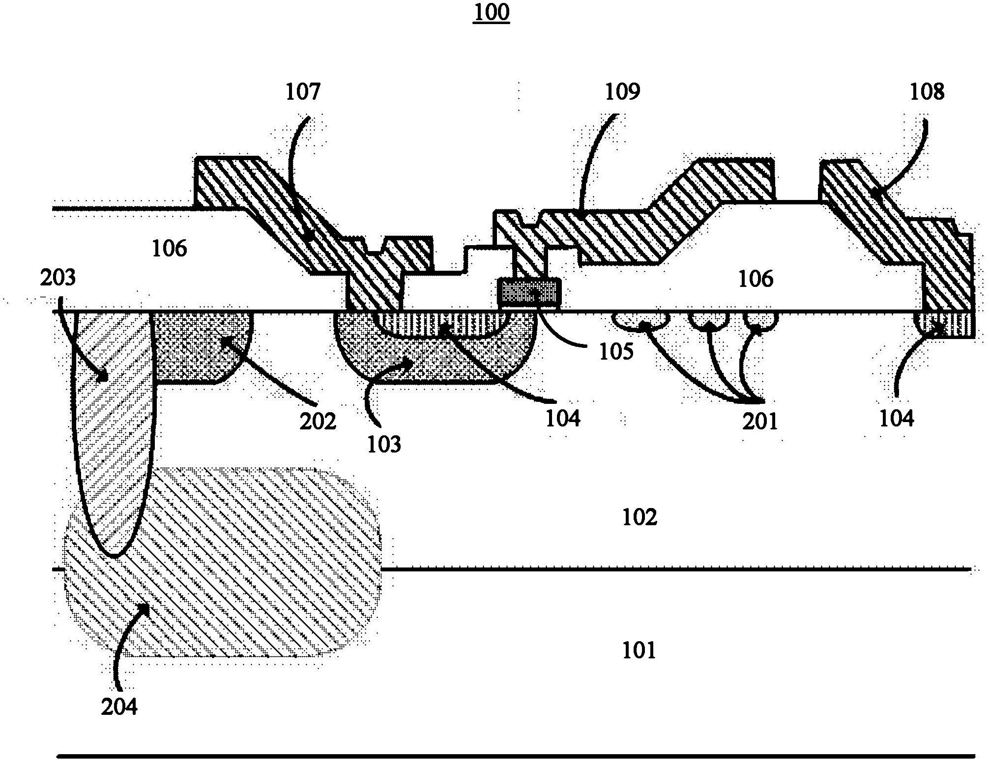
[0028] The present invention will be further described below in conjunction with specific embodiment and accompanying drawing, set forth more details in the following description so as to fully understand the present invention, but the present invention can obviously be implemented in many other ways different from this description, Those skilled in the art can make similar promotions and deductions based on actual application situations without violating the connotation of the present invention, so the content of this specific embodiment should not limit the protection scope of the present invention.

[0029] The present invention is applicable to various ultra-high voltage LDMOS gate metals, not limited to the LDMOS structure shown in this embodiment.

[0030] When the ultra-high voltage LDMOS structure is used in high-frequency switching applications, high breakdown voltage in the off state and low on-resistance in the on-state are the basic requirements. To obtain low on-re...


PUM


Abstract

The invention provides an LDMOS structure in an ultrahigh voltage BCD technology. The LDMOS structure is in an N-epitaxial layer on a P-substrate. Moreover, the LDMOS structure comprises: a first high voltage P type body region, which is at the N- epitaxial layer surface; two high voltage N+ injection regions, which are respectively at the first high voltage P type body region and a drain electrode position; a gate oxide and polysilicon gate, which is at the upper surface of the N-epitaxial layer and is connected with the first high voltage P type body region; an interlayer dielectric layer, which is covered on the upper surface of the N-epitaxial layer as well as is opened with windows at a source electrode position and the drain electrode position of the LDMOS structure and the polysilicon gate position; a source electrode field plate is arranged on the interlayer dielectric layer as well as is short-circuited with the first high voltage P type body region through the source electrode window; a drain source field plate, which is arranged on the interlayer dielectric layer as well as is connected with the drain electrode through the drain electrode window; and a gate field plate, which is arranged on the interlayer dielectric layer as well as is connected with the polysilicon gate through the gate window. According to the invention, the filed plates that can reduce surface electric fields and improve an overpressure resistant performance are provided; and moreover, parasitic resistance of the polysilicon gate can be substantially reduced; and gate switching frequency can be enhanced.

Description

technical field [0001] The invention relates to the technical field of semiconductor devices, in particular, the invention relates to an LDMOS structure in an ultra-high voltage BCD process. Background technique [0002] Ultra-high voltage LDMOS refers to a high-voltage double-diffused MOS structure with a lateral channel structure and a drift region, and a withstand voltage of 300V to 1200V. The drain, gate and source of this type of device are all located on the surface of the chip, and are usually made on the epitaxial silicon wafer. It is easy to realize isolation and signal connection with various low-voltage devices, and is an important part of realizing high-voltage integrated circuits (HVIC). device. When applied to the HVIC of power electronics, LDMOS is usually used as a switching device to switch back and forth between the on-state and the off-state, and to control a large power load with the minimum switching loss. This means that in addition to the requirement...

Claims


Application Information

Patent Timeline
Patent Type & Authority Applications(China)
IPC IPC(8): H01L29/78H01L29/40H01L29/49
CPCH01L29/7816H01L29/404
Inventor 吕宇强邵凯陈雪萌永福杨海波
Owner ADVANCED SEMICON MFG CO LTD
Why Eureka
Try Eureka