Row/column matrix keyboard interface circuit and row/column matrix keyboard scanning method
A matrix keyboard and interface circuit technology, applied in the field of circuits, can solve the problems of not saving I/O port resources, wasting I/O port resources, etc., and achieve simplified key scanning workload, high application value, and simple location Effect
- Summary
- Abstract
- Description
- Claims
- Application Information
AI Technical Summary
Problems solved by technology
Method used
Image
Examples
Embodiment 1
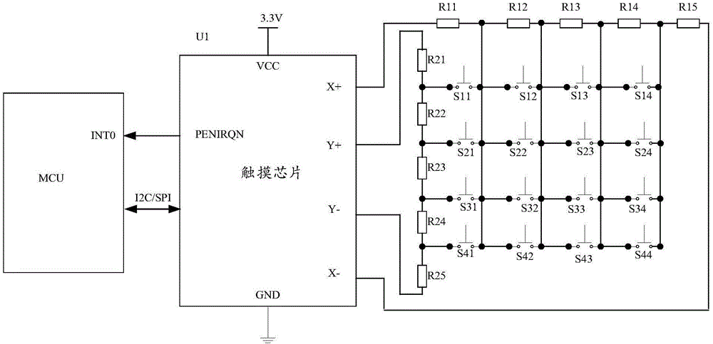
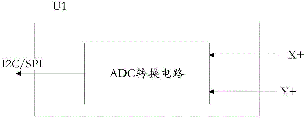
[0026] Embodiment 1, a row-column matrix keyboard interface circuit. see below figure 2 and image 3 The circuit provided by this embodiment is described.
[0027] see figure 2 The row-column matrix keyboard interface circuit provided in this embodiment includes a single-chip microcomputer MCU and a touch chip U1, the interrupt INT0 of the single-chip microcomputer MCU is connected to the pin PENIRQN of the touch chip U1, and the single-chip microcomputer MCU is connected to the touch chip U1 through the I2C / SPI bus , to realize the I2C / SPI communication between the MCU and the touch chip U1, the pin VCC is connected to the 3.3V power supply, and the pin GND is grounded. Connect m resistors in series between pin X+ and pin X- of the touch chip U1 as row resistors, and connect n resistors in series between pin Y+ and pin Y- as column resistors, between every two adjacent row resistors Lead out a column line, lead out a row line between every two adjacent column resistors,...
Embodiment 2
[0030] Embodiment 2, a scanning method of a row-column matrix keyboard. Combine below Figure 4-Figure 6 The scanning method provided in this embodiment is described.
[0031] see Figure 4 , the scanning method of the row-column matrix keyboard that the present embodiment provides comprises:
[0032] S1, the interrupt INT0 of the single-chip MCU generates an enabling drive signal to drive the touch chip U1 to work;
[0033] S2, when the button is pressed, the driving voltage V is applied to the pin X+ of the touch chip U1 Drive , pin X- is grounded to form a voltage gradient, and the output voltage V is measured at the terminal of pin Y+ xout ;
[0034] S3, apply the driving voltage V at the pin Y+ of the touch chip U1 Drive , pin Y- is grounded to form a voltage gradient, and the output voltage V is measured at the pin X+ terminal Yout ;
[0035] S4, the touch chip U1 will measure the obtained V xout and V Yout Transmit to single-chip MCU through I2C / SPI communicat...
PUM
 Abstract
Description
Claims
Application Information


