Copper Alloy Bonding Wire

A technology of copper alloy and bonding wire, which is applied in the direction of semiconductor/solid-state device parts, semiconductor devices, electrical components, etc., to achieve the effect of stable position, stable shape, and shortened bonding step time

Inactive Publication Date: 2020-03-03
TANAKA DENSHI KOGYO KK
View PDF8 Cites 0 Cited by
  • Summary
  • Abstract
  • Description
  • Claims
  • Application Information

AI Technical Summary

Problems solved by technology

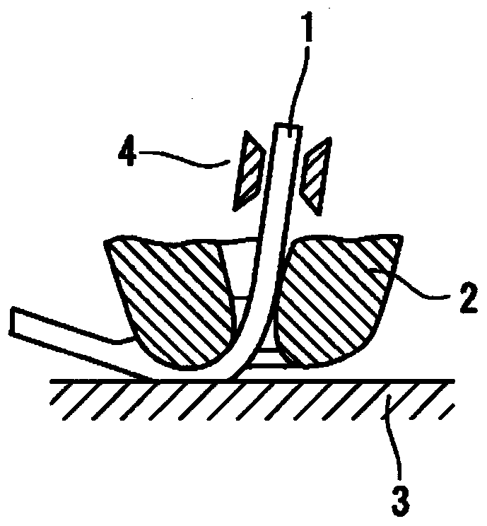
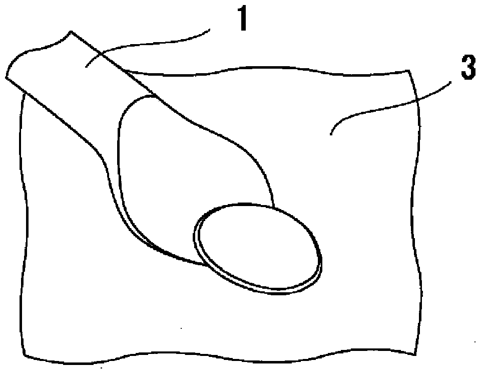
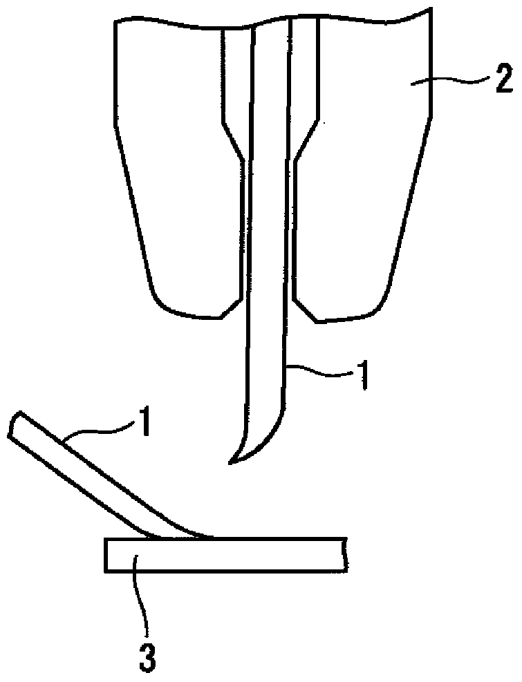
[0018] The present invention is used to solve the following technical problem: in the wedge welding step of pulling up the copper alloy bonding wire directly after wedge welding to cut off such a second joint in the shortest time, the front end of the wire is deformed into a J shape

Method used


Image

  • Copper Alloy Bonding Wire
  • Copper Alloy Bonding Wire
  • Copper Alloy Bonding Wire

Examples


Embodiment

[0062] The core material uses copper (Cu) with a purity of 99.9998% by mass (5N), and phosphorus (P) and nickel (Ni), palladium (Pd), platinum (Pt), gold (Au) and silver (Ag) as an added element. As the base metal element, an element generally contained in high-purity copper is selected. That is, bismuth (Bi), selenium (Se), tellurium (Te), zinc (Zn), iron (Fe), nickel (Ni), and tin (Sn) are appropriately selected. Embodiments in which these metals are blended within predetermined ranges are referred to as Example 1 to Example 5, respectively.

[0063] Next, it was melted and continuously cast, and then the first wire drawing was performed within the range of 95-99.99% or less in section reduction to obtain a thick wire (diameter: 1.0 mm) before being covered with a drawing material. Next, perform intermediate heat treatment (300-600° C. for 0.5-3 hours) (Example 4, Example 5) or not perform intermediate heat treatment (Example 1-Example 3). Afterwards, thin extension l...


PUM

PropertyMeasurementUnit
diameteraaaaaaaaaa

Abstract

The invention provides a copper alloy bonding wire, the copper alloy crystal grains per unit cross-sectional area are 50-250, the maximum grain size is less than 1 / 3 of the diameter of the bonding wire, and the specific direction is less than 40%. of no directionality.

Description

technical field [0001] The present invention relates to a copper alloy bonding wire suitable for connecting an electrode of an IC chip used in a semiconductor device to a substrate such as an external lead frame. Background technique [0002] In general, a method called ball bonding is used for the first bonding of copper bonding wires and electrodes, and a method called wedge bonding is used for bonding copper bonding wires and wiring on a circuit wiring board for semiconductors. For wedge welding. The first bonding is to apply a thermal arc from a torch electrode to the tip of the wire in the form of electronic frame off (EFO), so that the tip of the wire forms a positive ball called a solder ball (FAB). Next, ultrasonic waves (ultrasonic waves) are applied while pressing this FAB onto an aluminum pad heated in a temperature range of 150 to 300° C. by a capillary, so that a bonding wire is bonded to the aluminum pad. [0003] Next, the solder pin is raised while pulling ...

Claims


Application Information

Patent Timeline
Patent Type & Authority Patents(China)
IPC IPC(8): H01L23/49H01L23/498
CPCH01L23/49811H01L24/45H01L23/49H01L2224/45139H01L2224/45147H01L2224/45144H01L2224/45163H01L2224/78301H01L2224/85H01L2924/00011H01L2224/45565H01L2224/45572H01L2224/45644H01L2224/45664H01L2224/48247H01L2224/48451H01L2224/48456H01L2224/85439H01L2224/43848H01L2924/01079H01L2924/01047H01L2924/01015H01L2924/01028H01L2924/01046H01L2924/01078H01L2924/013H01L2924/01026H01L2924/0103H01L2924/01034H01L2924/0105H01L2924/01052H01L2924/01083H01L2924/00013H01L2924/01033H01L2924/01206H01L2924/01049
Inventor 天野裕之三苫修一滨本拓也
Owner TANAKA DENSHI KOGYO KK
Why Eureka
Try Eureka