
Flexible circuit board and manufacturing method therefor

A technology of flexible circuit boards and manufacturing methods, which is applied to printed circuits, printed circuits, printed circuits connected with non-printed electrical components, etc., can solve the problems of multiple signal reflections, signal transmission energy loss, etc., and reduce signal transmission. Loss, avoiding the effect of impedance discontinuity

Active Publication Date: 2017-03-08
AVARY HLDG (SHENZHEN) CO LTD +2
View PDF4 Cites 2 Cited by
  • Summary
  • Abstract
  • Description
  • Claims
  • Application Information

AI Technical Summary

Problems solved by technology

[0002] In the environment of rapid development of information transmission, high-frequency signal transmission needs to have higher transmission requirements, and then the flexible circuit board used for high-frequency signal transmission plays an increasingly important role in electronic circuits. Generally, if the signal The transmission line is located in the inner layer of the flexible circuit board, and the line needs to be led out to the outer layer through conductive blind holes to mount parts, and the existence of the blind hole will cause multiple reflections of the signal, resulting in energy loss during signal transmission

Method used


Image

  • Flexible circuit board and manufacturing method therefor
  • Flexible circuit board and manufacturing method therefor
  • Flexible circuit board and manufacturing method therefor

Examples


Embodiment Construction

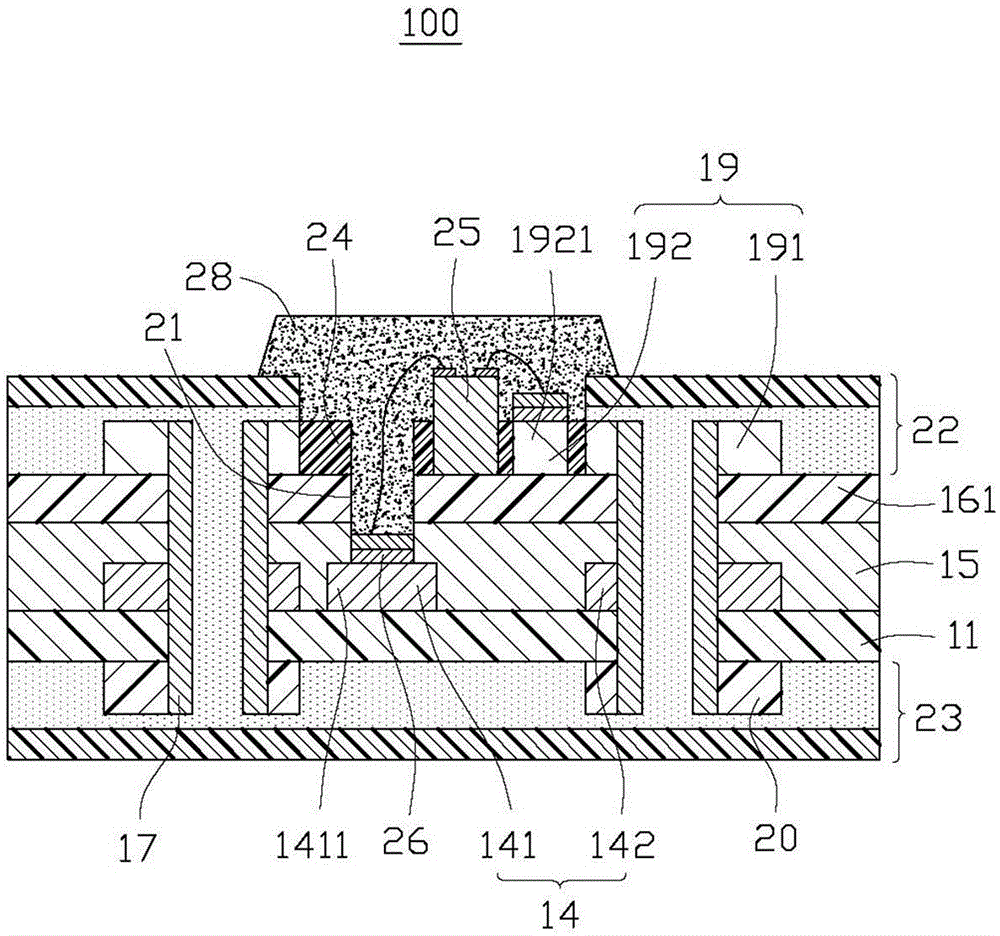
[0025] see figure 1 , Figure 9 and Figure 13 , the first embodiment of the present invention provides a flexible circuit board 100 for high-frequency signal transmission, including: an inner conductive circuit layer 14, a first conductive circuit layer 19 formed on opposite sides of the inner conductive circuit layer 14 and The second conductive circuit layer 20, the second insulating layer 161 and the glue layer 15 formed between the first conductive circuit layer 19 and the inner conductive circuit layer 14, the second conductive circuit layer 20 and the The first insulating layer 11 between the inner conductive circuit layers 14, the first covering film layer 22 formed on the side of the first conductive circuit layer 19 away from the second conductive circuit layer 20, and the first covering film layer 22 formed on the side of the first conductive circuit layer 19 The second conductive circuit layer 20 is away from the second cover film layer 23 , solder resist layer 2...


PUM


Abstract

The invention discloses a flexible circuit board used for high-frequency signal transmission. The flexible circuit board comprises an inner layer conductive circuit layer, a first conductive circuit layer, a second conductive circuit layer, a window, and an electronic element, wherein the inner layer conductive circuit layer comprises a signal transmission line; a first welding pad is defined at one end part of the signal transmission line; the first conductive circuit layer is formed on one side of the inner layer conductive circuit layer; the first conductive circuit layer comprises a conductive circuit; a second welding pad is defined on the conductive circuit; the projection of the second welding pad on the inner layer conductive circuit layer is staggered from the first welding pad of the signal transmission line; the second conductive circuit layer is formed on the other side of the inner layer conductive circuit layer; at least one part of the first welding pad is exposed out of the window; and the electrodes of the electronic element are electrically connected with the first welding pad and the second welding pad separately. The invention also relates to a manufacturing method for the flexible circuit board.

Description

technical field [0001] The invention relates to the field of circuit board production, in particular to a flexible circuit board for high-frequency signal transmission and a production method thereof. Background technique [0002] In the environment of rapid development of information transmission, high-frequency signal transmission needs to have higher transmission requirements, and then the flexible circuit board used for high-frequency signal transmission plays an increasingly important role in electronic circuits. Generally, if the signal The transmission line is located in the inner layer of the flexible circuit board, and the line needs to be led out to the outer layer through conductive blind holes to mount parts, and the existence of the blind hole will cause multiple reflections of the signal, resulting in energy loss during signal transmission. Contents of the invention [0003] Therefore, it is necessary to provide a flexible circuit board for high-frequency sig...

Claims


Application Information

Patent Timeline
Patent Type & Authority Applications(China)
IPC IPC(8): H05K1/18
CPCH05K1/183H05K2201/09427H05K2201/09472
Inventor 胡先钦李艳禄王凯游文信何明展
Owner AVARY HLDG (SHENZHEN) CO LTD
Learn More