Array substrate and display panel

An array substrate and display panel technology, applied in nonlinear optics, instruments, optics, etc., can solve problems such as large impedance difference and uneven display

Active Publication Date: 2017-03-22
XIAMEN TIANMA MICRO ELECTRONICS +1
View PDF6 Cites 14 Cited by
  • Summary
  • Abstract
  • Description
  • Claims
  • Application Information

AI Technical Summary

Problems solved by technology

[0004] The present invention provides an array substrate and a display panel to solve the proble

Method used


Image

  • Array substrate and display panel
  • Array substrate and display panel
  • Array substrate and display panel

Examples


Embodiment Construction

[0019] The present invention will be further described in detail below in conjunction with the accompanying drawings and embodiments. It should be understood that the specific embodiments described here are only used to explain the present invention, but not to limit the present invention. In addition, it should be noted that, for the convenience of description, only some structures related to the present invention are shown in the drawings but not all structures.

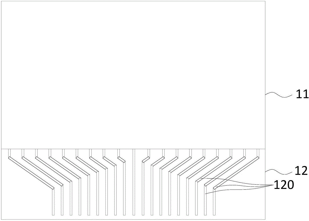
[0020] An embodiment of the present invention provides an array substrate, the array substrate includes a display area and a non-display area, and the non-display area is provided with a plurality of connecting leads;

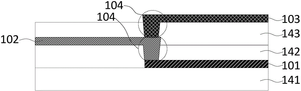
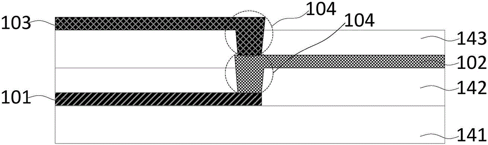
[0021] The connecting leads include a plurality of first connecting leads, the first connecting leads include a first metal wiring, a second metal wiring and a third metal wiring, and the first metal wiring, the second metal wiring and the third metal wiring At least two of them are located in diff...


PUM


Abstract

The embodiment of the invention discloses an array substrate and a display panel. The array substrate comprises a display area and a non-display area. The non-display area is provided with a plurality of connecting leads, the connecting leads comprise a plurality of first connecting lead bodies, the first connecting lead bodies comprise first metal wirings, second metal wirings and third metal wirings, and at least two metal wirings of the first metal wirings, the second metal wirings and the third metal wirings are located on different film layers. By means of the array substrate and the display panel in the embodiment, the signal transmission uniformity in the different connecting leads is improved, and the display panel is even in display.

Description

technical field [0001] Embodiments of the present invention relate to the field of display technologies, and in particular, to an array substrate and a display panel. Background technique [0002] The liquid crystal display panel has an effective display area and a non-display area. A plurality of pixels are arranged in the effective display area to form a pixel array, and peripheral circuits are provided in the non-display area. Each pixel generally includes at least one thin film transistor and a pixel electrode connected to the thin film transistor, and each pixel is surrounded by two adjacent scan lines and two adjacent data lines. These scan lines and data lines extend from the effective display area to the non-display area, and are electrically connected to the driving chip through the peripheral lines of the non-display area. The peripheral lines are fan-out lines formed by concentrating one end connecting the scan line and the data line to the area where the driver...

Claims


Application Information

Patent Timeline
IPC IPC(8): G02F1/1345
CPCG02F1/13452
Inventor 刘冰萍周秀峰李俊谊
Owner XIAMEN TIANMA MICRO ELECTRONICS
Why Eureka
Try Eureka