Pixel circuit compensation method, OLED display panel and compensation method thereof

A technology of pixel circuit and compensation method, applied in static indicators, instruments, etc., can solve problems such as threshold voltage changes of OLED devices

Inactive Publication Date: 2017-03-22
SHANGHAI TIANMA AM OLED +1
View PDF10 Cites 5 Cited by
  • Summary
  • Abstract
  • Description
  • Claims
  • Application Information

AI Technical Summary

Problems solved by technology

[0006] Embodiments of the present invention provide a compensation method for a pixel circuit, an OLED display panel and a compensation method t

Method used


Image

  • Pixel circuit compensation method, OLED display panel and compensation method thereof
  • Pixel circuit compensation method, OLED display panel and compensation method thereof
  • Pixel circuit compensation method, OLED display panel and compensation method thereof

Examples


Embodiment Construction

[0023] The specific implementation manners of the compensation method for the pixel circuit, the OLED display panel and the compensation method thereof provided by the embodiments of the present invention will be described in detail below with reference to the accompanying drawings.

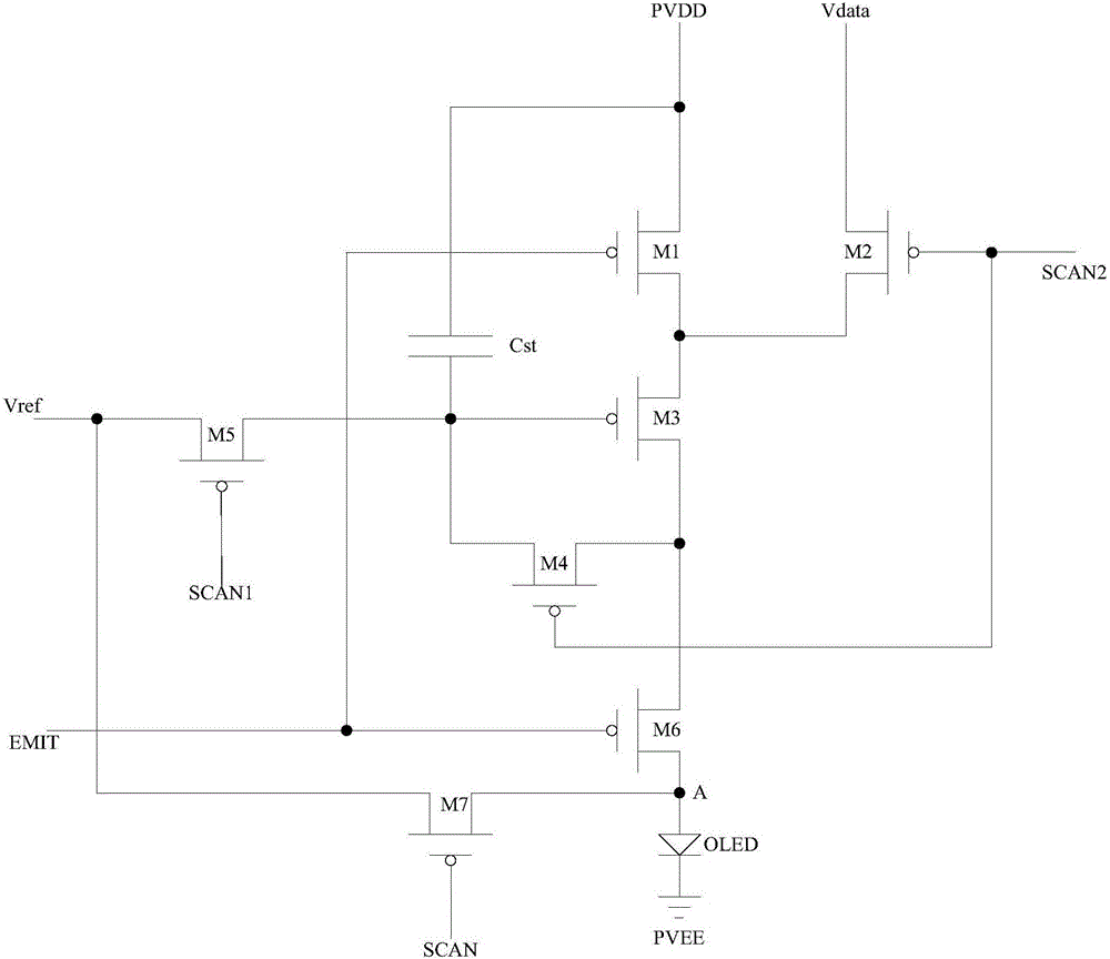
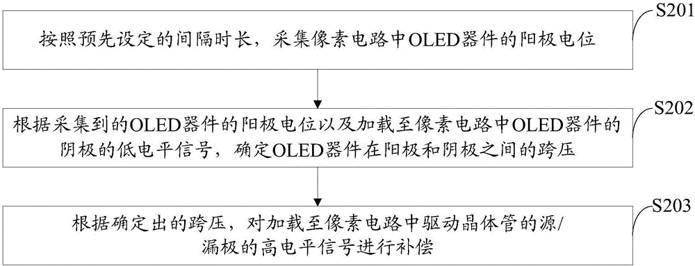
[0024] An embodiment of the present invention provides a compensation method for a pixel circuit, such as figure 2 shown, including the following steps:

[0025] S201. Collect the anode potential of the OLED device in the pixel circuit according to the preset interval, that is, collect as figure 1 The potential Vt of point A in the pixel circuit shown; in specific implementation, a separate acquisition signal line can be added in the pixel circuit for potential acquisition;

[0026] S202. According to the collected anode potential of the OLED device and the low-level signal loaded to the cathode of the OLED device in the pixel circuit, determine the cross voltage of the OLED device between the ...


PUM


Abstract

The invention discloses a pixel circuit compensation method, an OLED display panel and a compensation method thereof. The cross voltage of an OLED device between the anode and the cathode is determined by acquiring the anode potential of the OLED device in at least one pixel circuit of at least one color in the OLED display panel so as to compensate high-level signals loaded to the source/drain electrode of driving transistors in each pixel circuit of the color. The current of the OLED device increases along with attenuation of the OLED device in use, and the cross voltage change of the OLED device caused by the life attenuation of the OLED device is compensated to the high-level signals loaded to drive the source/drain electrodes of all the driving transistors of the OLED device of the color so as to improve the ghosting phenomenon.

Description

technical field [0001] The invention relates to the display field, in particular to a compensation method for a pixel circuit, an OLED display panel and a compensation method thereof. Background technique [0002] With the advancement of display technology, more and more active matrix organic light emitting diode (Active Matrix Organic Light Emitting Diode, AMOLED) display panels have entered the market, compared with traditional transistor liquid crystal display panels (Thin Film Transistor Liquid Crystal Display, TFT LCD) In comparison, it has the advantages of low energy consumption, low production cost, self-illumination, wide viewing angle, and fast response speed. At present, it has gradually replaced traditional LCD displays in the display fields of mobile phones, PDAs, and digital cameras. Unlike TFT LCD, which uses a stable voltage to control brightness, AMOLED is current-driven and requires a stable current to control light emission. [0003] There are many existi...

Claims


Application Information

Patent Timeline
IPC IPC(8): G09G3/3258
CPCG09G3/3258
Inventor 范刘静刘海民
Owner SHANGHAI TIANMA AM OLED
Why Eureka
Try Eureka