Display device, pixel circuit and control method thereof

A technology of pixel circuit and capacitor, applied in the field of liquid crystal display, can solve the problem of afterimage contrast and other problems of display screen

Active Publication Date: 2019-11-29
BOE TECH GRP CO LTD +1
View PDF7 Cites 0 Cited by
  • Summary
  • Abstract
  • Description
  • Claims
  • Application Information

AI Technical Summary

Problems solved by technology

[0005] In view of this, the object of the present invention is to provide a display device, a pixel circuit and a control method thereof, which are used to improve the hysteresis characteristics of the pixel circuit and reduce the leakage current, thereby improving the afterimage problem and the low contrast problem of the display screen

Method used


Image

  • Display device, pixel circuit and control method thereof
  • Display device, pixel circuit and control method thereof
  • Display device, pixel circuit and control method thereof

Examples


Embodiment 1

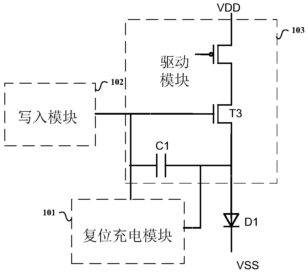
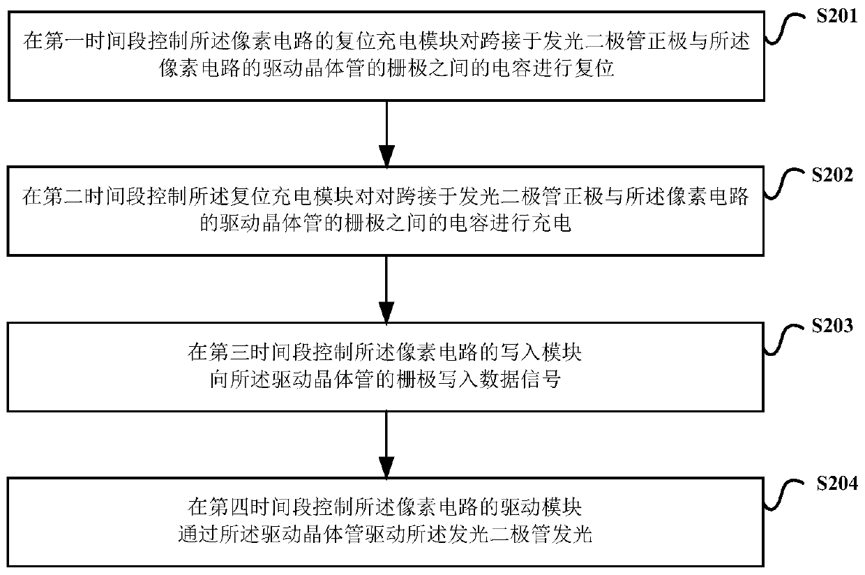
[0080] The pixel circuit provided by Embodiment 1 of the present invention is as follows image 3 As shown, the driving module therein is specifically configured to drive the light emitting diode to emit light through the driving transistor according to the valid signal of the light emitting indication signal EM arriving in the fourth time period.

[0081] Specifically, the driving module in the pixel circuit of Embodiment 1 of the present invention may include an input port of a light-emitting indication signal, which is the input port of the light-emitting indication signal of the pixel circuit, and is connected to the light-emitting indication signal line; It may also include: a capacitor C1, the driving transistor T3 and the transistor T4 connected in series between the device operating voltage VDD and the anode of the light emitting diode D1. The cathode of the LED D1 is connected to the common ground voltage VSS.

[0082] For ease of description, the connection point be...

Embodiment 2

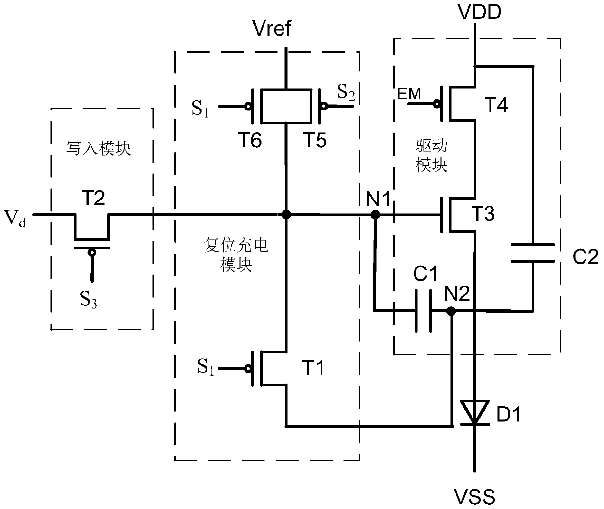
[0106] like Image 6 As shown, the circuit structures of the driving module and the writing module in the pixel circuit provided by the second embodiment of the present invention are the same as the circuit structures of the driving module and the writing module in the pixel circuit of the first embodiment of the present invention, and are not repeated here. repeat.

[0107] The reset charging module in the pixel circuit provided by Embodiment 2 of the present invention is specifically used to reset the capacitor according to the valid signals of the first and second timing signals arriving in the first time period, and according to the second A valid signal of the timing signal charges the capacitor.

[0108] Specifically, the reset charging module in the pixel circuit provided by Embodiment 2 of the present invention includes: input ports that may include first and second timing signals, which are respectively used as input ports of the first and second timing signals of th...

Embodiment 3

[0122] like Figure 9 As shown, the circuit structures of the driving module and the writing module in the pixel circuit provided by the third embodiment of the present invention are respectively the same as the circuit structures of the driving module and the writing module in the pixel circuit of the first embodiment of the present invention, and are not repeated here. repeat.

[0123] The reset charging module in the pixel circuit provided by Embodiment 3 of the present invention is specifically used to reset the capacitor according to the valid signals of the first and second timing signals arriving in the first time period, and according to the second timing signal extended in the second time period. A valid signal of the timing signal charges the capacitor.

[0124] Specifically, the reset charging module in the pixel circuit provided by the third embodiment of the present invention may include the input ports of the first and second timing signals, which are respective...


PUM


Abstract

The invention discloses a display device, a pixel circuit and a control method thereof. The circuit comprises: a reset charging module, which is used for charging a capacitance between a gate of a driving transistor connected across the pixel circuit and a positive electrode of a light-emitting diode. After resetting, the capacitor is charged; a writing module is used to write a data signal to the gate of the driving transistor; a driving module includes the driving transistor and is used to receive the data signal at the driving transistor When driving the light emitting diode to emit light; wherein, the driving transistor used for driving the light emitting diode to emit light adopts oxide TFT, and other transistors in the pixel circuit adopt LTPS TFT. The invention can improve the hysteresis characteristic of the pixel circuit and reduce the leakage current, thereby improving the problem of afterimage and low contrast of the display screen.

Description

technical field [0001] The present invention relates to the technical field of liquid crystal display, in particular to a display device, a pixel circuit and a control method thereof. Background technique [0002] Among various types of flat-panel display devices, active matrix organic light-emitting display devices (AMOLED) use self-luminous organic light-emitting diodes (OLEDs) to display images, usually have a short response time, use low power consumption for driving, and are relatively more Due to the characteristics of good brightness and color purity, organic light emitting display devices have become the focus of next generation display devices. [0003] For a large-scale active matrix organic light emitting display device, it includes a plurality of pixels located at the crossing regions of scan lines and data lines. Each pixel includes an organic light emitting diode and a pixel circuit for driving the organic light emitting diode. A pixel circuit usually include...

Claims


Application Information

Patent Timeline
Patent Type & Authority Patents(China)
IPC IPC(8): G09G3/3275G09G3/3225
CPCG09G3/3225G09G3/3275G09G2320/0257G09G3/3233G09G3/3266G09G2300/0814G09G2300/0819G09G2300/0852G09G2300/0861G09G2310/08G09G2320/066G09G3/2092G09G3/32G09G2310/0272
Inventor 冯宇刘利宾
Owner BOE TECH GRP CO LTD
Why Eureka
Try Eureka