Packaging-free high-luminance LED chip structure and manufacturing method therefor
A technology of LED chip and LED structure, which is applied in the direction of electrical components, circuits, semiconductor devices, etc., can solve the problems of large leakage rate of flip chip structure, increase of production cost, increase of process steps, etc., to save packaging process and reduce leakage rate , good transmittance effect
- Summary
- Abstract
- Description
- Claims
- Application Information
AI Technical Summary
Problems solved by technology
Method used
Image

Examples
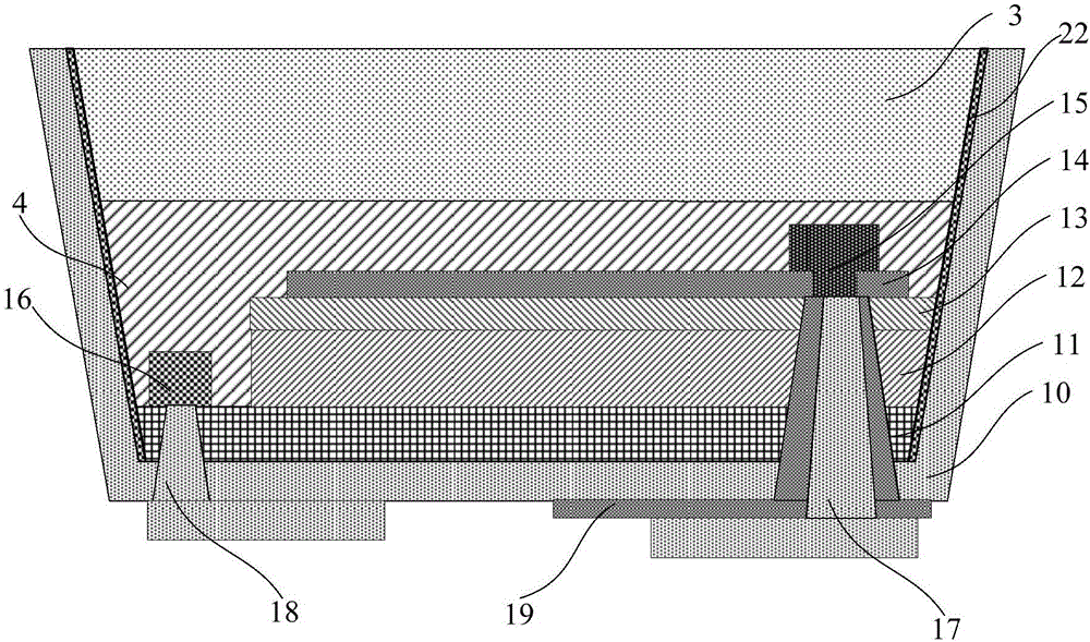
Embodiment 1
[0064] see figure 1 , the present invention provides a package-free high-brightness LED chip structure. The present invention provides a package-free high-brightness LED chip structure. The package-free high-brightness LED chip structure includes: a GaN-based LED structure and a transparent substrate 3; The GaN-based LED structure includes a reflector 10, an N-type GaN layer 11, a light-emitting layer 12, a P-type GaN layer 13, a transparent electrode 14, a P electrode 15, an N electrode 16, and a P electrode lead-out electrode 17; the reflector 10, the The N-type GaN layer 11, the light-emitting layer 12, the P-type GaN layer 13, and the transparent electrode 14 are sequentially stacked from bottom to top; the side of the GaN-based LED structure away from the reflector 10 is a P-side The P electrode 15 runs through the transparent electrode 14 and is in contact with the P-type GaN layer 13, that is, one end of the P electrode is located on the surface of the P-type GaN layer ...
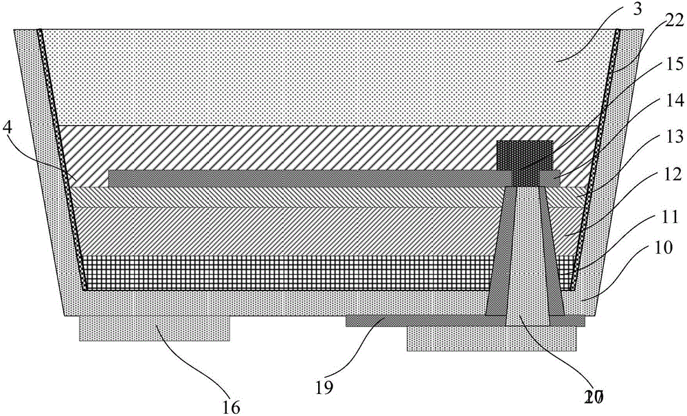
Embodiment 2
[0072] see figure 2 , this embodiment also provides a package-free high-brightness LED chip structure, the package-free high-brightness LED chip structure includes: a GaN-based LED structure and a transparent substrate 3; the GaN-based LED structure includes a reflector 10, an N-type GaN layer 11, light-emitting layer 12, P-type GaN layer 13, transparent electrode 14, P-electrode 15, N-electrode 16, and P-electrode lead-out electrode 17; the mirror 10, the N-type GaN layer 11, the light-emitting layer 12. The P-type GaN layer 13 and the transparent electrode 14 are stacked sequentially from bottom to top; the side of the GaN-based LED structure away from the reflector is the P surface; the P electrode 15 runs through the transparent electrode 14 And it is in contact with the P-type GaN layer 13, that is, one end surface of the P-type electrode is located on the surface of the P-type GaN layer 13, and the other end extends through the transparent electrode 14 to above the tran...
Embodiment 3
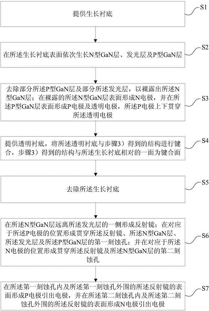
[0079] see image 3 , the present invention also provides a method for manufacturing a package-free high-brightness LED chip structure, the method is suitable for preparing the package-free high-brightness LED chip structure in Example 1, and the method includes the following steps:
[0080] 1) Provide a growth substrate;
[0081] 2) sequentially growing an N-type GaN layer, a light-emitting layer and a P-type GaN layer on the surface of the growth substrate;
[0082] 3) removing part of the P-type GaN layer and part of the light-emitting layer to expose the N-type GaN layer; forming an N electrode on the exposed surface of the N-type GaN layer, and forming an N electrode on the surface of the P-type GaN layer forming a P electrode and a transparent electrode, and the P electrode penetrates the transparent electrode up and down;
[0083] 4) providing a transparent substrate, bonding the transparent substrate to the structure obtained in step 3), the side opposite to the grow...
PUM
 Abstract
Description
Claims
Application Information
 - R&D
- Intellectual Property
- Life Sciences
- Materials
- Tech Scout
- Unparalleled Data Quality
- Higher Quality Content
- 60% Fewer Hallucinations
Browse by: Latest US Patents, China's latest patents, Technical Efficacy Thesaurus, Application Domain, Technology Topic, Popular Technical Reports.
© 2025 PatSnap. All rights reserved.Legal|Privacy policy|Modern Slavery Act Transparency Statement|Sitemap|About US| Contact US: help@patsnap.com