Least switching loss implementation method of three-level inverter

A three-level inverter, switching loss technology, applied in the field of power electronics, can solve problems such as unsatisfactory results

Inactive Publication Date: 2017-03-22
UNIV OF ELECTRONICS SCI & TECH OF CHINA
View PDF6 Cites 10 Cited by
  • Summary
  • Abstract
  • Description
  • Claims
  • Application Information

AI Technical Summary

Problems solved by technology

Although DPWM can clamp the output level of the switching tube to a certain extent, so that the switching loss is reduced, DPWM has many types of modulation strategies, which can better reduce the switching loss in the specific modulation ratio and power factor angle range. loss, but not ideal for all modulation ratios and power factor angular ranges

Method used


Image

  • Least switching loss implementation method of three-level inverter
  • Least switching loss implementation method of three-level inverter
  • Least switching loss implementation method of three-level inverter

Examples


Embodiment

[0104] For the convenience of description, the relevant technical terms appearing in the specific implementation are explained first:

[0105] PWM (Pulse Width Modulation): pulse width modulation;

[0106] IGBT (Insulated Gate Bipolar Transistor): insulated gate bipolar transistor;

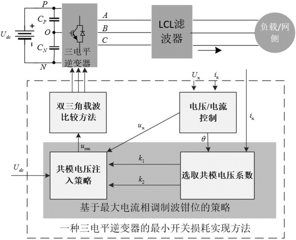
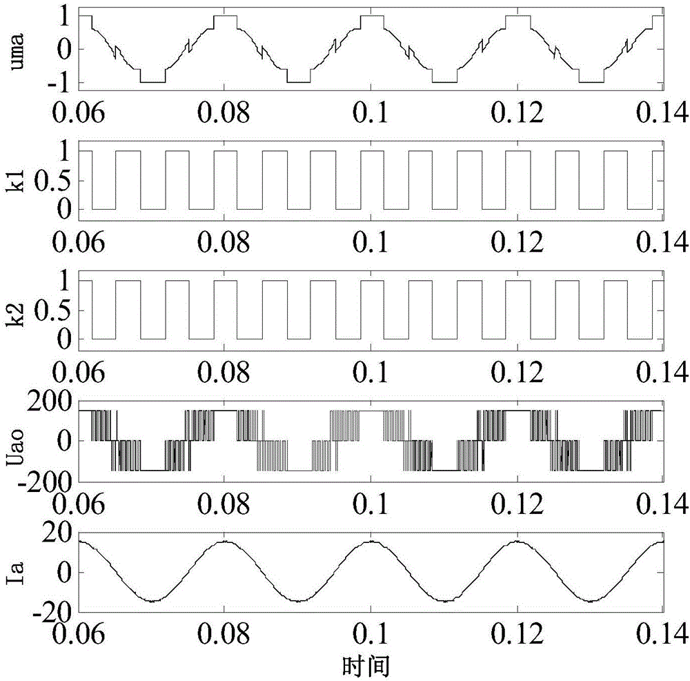
[0107] figure 1 It is a block diagram of a method for realizing the minimum switching loss of a three-level inverter in the present invention.

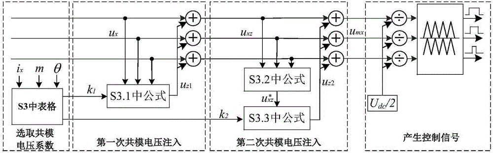
[0108] In this example, combined with figure 1 The block diagram of a minimum switching loss realization method of a three-level inverter is shown, and the three-level minimum switching loss method is described in detail, including the following steps:

[0109] S1. Obtain the AC side voltage U through the voltage and current sensor x (x=a,b,c), AC side current i x (x=a,b,c), total DC side voltage U dc real-time data.

[0110] S2, combined with AC side current i x , AC side voltage U x Get the three-phase voltage control signal u through voltage a...


PUM


Abstract

The present invention discloses a least switching loss implementation method of a three-level inverter. According to the data of alternating current side voltage, the alternating current side current and the direct current side total voltage collected by a sensor and the region whether the current relation and the voltage vectors are located, a common-mode voltage coefficient k1 and a common-mode voltage coefficient k2 are selected, the equivalent modulation wave based on the maximum current phase modulation wave clamping is calculated, and the IGBT driving signals are generated through adoption of the double-triangle carrier comparison method. Through combination of the strategy of the maximum current phase modulation wave clamping and the double-triangle carrier comparison method, the least switching loss method is realized.

Description

technical field [0001] The invention belongs to the technical field of power electronics, and more specifically relates to a method for realizing the minimum switching loss of a three-level inverter. Background technique [0002] In recent years, three-level inverters have been developed rapidly. The modulation strategies mainly used in three-level inverters include sinusoidal pulse width modulation (SPWM), space vector pulse width modulation (SVPWM), and discontinuous pulse width modulation. Modulation (DPWM), etc. In SPWM and SVPWM, the switching tube is operating in every switching cycle, so a very large switching loss is generated. Although DPWM can clamp the output level of the switching tube to a certain extent, so that the switching loss is reduced, DPWM has many types of modulation strategies, which can better reduce the switching loss within a specific modulation ratio and power factor angle range. losses, but is not ideal for all modulation ratios and power facto...

Claims


Application Information

Patent Timeline
Patent Type & Authority Applications(China)
IPC IPC(8): H02M7/537H02M7/5395
CPCH02M7/537H02M7/5395H02M1/0054Y02B70/10
Inventor 李凯魏旻邹见效郑宏徐红兵
Owner UNIV OF ELECTRONICS SCI & TECH OF CHINA
Why Eureka
Try Eureka