Check patentability & draft patents in minutes with Patsnap Eureka AI!

Circuit arrangement and method for addressing leds in a matrix configuration

A circuit device and bias device technology, applied in the field of circuit devices and methods for operating LEDs in a matrix configuration, can solve problems such as material creep, flicker, etc.

Active Publication Date: 2017-03-22
BSH BOSCH & SIEMENS HAUSGERAETE GMBH
View PDF6 Cites 0 Cited by
  • Summary
  • Abstract
  • Description
  • Claims
  • Application Information

AI Technical Summary

Problems solved by technology

The problem of material creep would thus be eliminated, but LED 21 and LED 12 could flicker more or less strongly depending on the color due to the applied voltage in the flow direction

Method used


Image

  • Circuit arrangement and method for addressing leds in a matrix configuration
  • Circuit arrangement and method for addressing leds in a matrix configuration
  • Circuit arrangement and method for addressing leds in a matrix configuration

Examples


Embodiment Construction

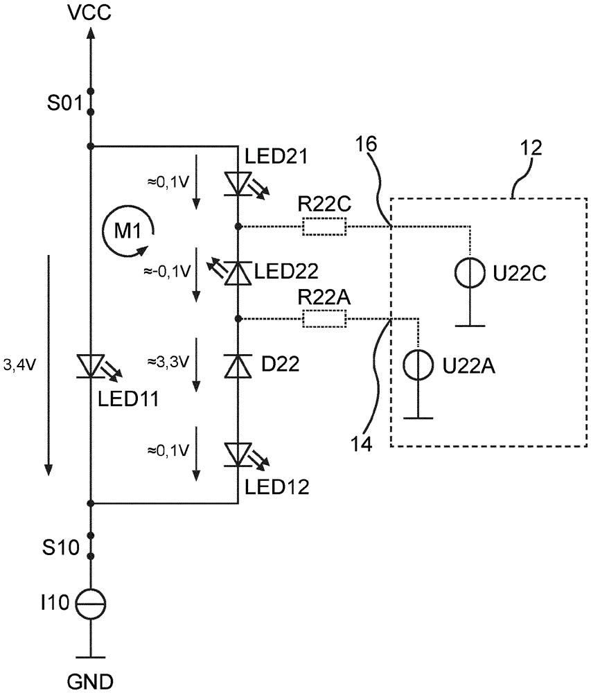
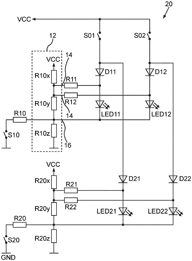
[0025] Then according to figure 1 to explain an exemplary LED matrix in a 2x2 configuration. Starting from a common reference potential GND, the first current source I10 and the second current source I20 are each coupled via a switch S10 or S20 to a row controller of the LED matrix. In this case, the switch S10 of the first row controller is connected to the negative pole of the LED 11 and the negative pole of the LED 12 . In addition, the switch S20 of the second row of manipulators is connected to the cathode of the LED 21 and the cathode of the LED 22 . In addition, the anodes of the LED11 and the LED21 are coupled to the power supply potential VCC through the switch S01 of the first column controller. Furthermore, the anodes of LED12 and LED22 are coupled to supply potential VCC via switch S02 of the second column operator. Thus, for example, a current flow through the LED 11 results when the switch S01 of the column manipulator is closed and when the switch S10 of the ...


PUM


Abstract

The invention relates to a circuit arrangement for addressing LEDs in a matrix configuration having m columns and n rows, wherein each LED (LED11, LED12, LED21, LED22) of the matrix can be individually addressed by the actuation of a corresponding column driver (S01, S02) in conjunction with the actuation of a corresponding row driver (S10, S20), with a bias system (12) for each row. The bias system (12) comprises a first bias connection (14) for electrically coupling to the cathodes of m LEDs (LED11, LED12) of the row and a second bias connection (16) for electrically coupling to the anodes of m LEDs (LED11, LED12) of the row, each LED (LED11, LED12, LED21, LED22) of the matrix being coupled to the connection of a column addressing system (S01, S02) by respective semiconductor diodes (D11, D12, D21, D22), and in addition, n semiconductor diodes (D11, D21) associated with the same column are each electrically interconnected at one of their respective electrodes. The invention further relates to a display device and to a household appliance having such a circuit arrangement, and to a method for addressing LEDs in a matrix configuration.

Description

technical field [0001] The invention relates to a circuit arrangement for actuating light-emitting diodes (Light-Emitting Diodes, LEDs for short) in a matrix configuration, wherein each LED of the matrix can be actuated individually by activating a corresponding column driver in combination with a corresponding row driver, wherein Furthermore, there is one biasing device per row, said biasing device having a first biasing connection terminal electrically coupled to the negative pole of the LEDs of the corresponding row and a second biasing connection terminal for being electrically coupled to the positive pole of the LEDs of the corresponding row. Set the connection terminal. Background technique [0002] In the case of LEDs in a matrix arrangement, a blocking voltage is applied to the LEDs in a defined state of the actuation within principle limits. figure 1 A 2x2 matrix (2 by 2 matrix) is shown as the simplest example. The blocking current flowing here (drawn in dashed l...

Claims


Application Information

Patent Timeline
Patent Type & Authority Applications(China)
IPC IPC(8): H05B33/08H05B44/00H05B45/50H05B45/59
CPCH05B45/50H05B45/46H05B45/59H05B45/00H05B44/00
Inventor M.巴尔布M.格哈特S.胡夫K-H.施托罗贝尔
Owner BSH BOSCH & SIEMENS HAUSGERAETE GMBH
Features
  • R&D
  • Intellectual Property
  • Life Sciences
  • Materials
  • Tech Scout
  • Unparalleled Data Quality
  • Higher Quality Content
  • 60% Fewer Hallucinations
Learn More