

Nitride semiconductor light emitting element and method for manufacturing same
一种氮化物类、发光元件的技术,应用在半导体/固态器件制造、半导体器件、电气元件等方向,达到抑制非均匀应变分布的效果
- Summary
- Abstract
- Description
- Claims
- Application Information
AI Technical Summary
Problems solved by technology
Method used
Image

Examples
Embodiment approach 1
[0089] First, refer to figure 1 A first embodiment of the nitride-based semiconductor light-emitting device according to the present invention will be described.
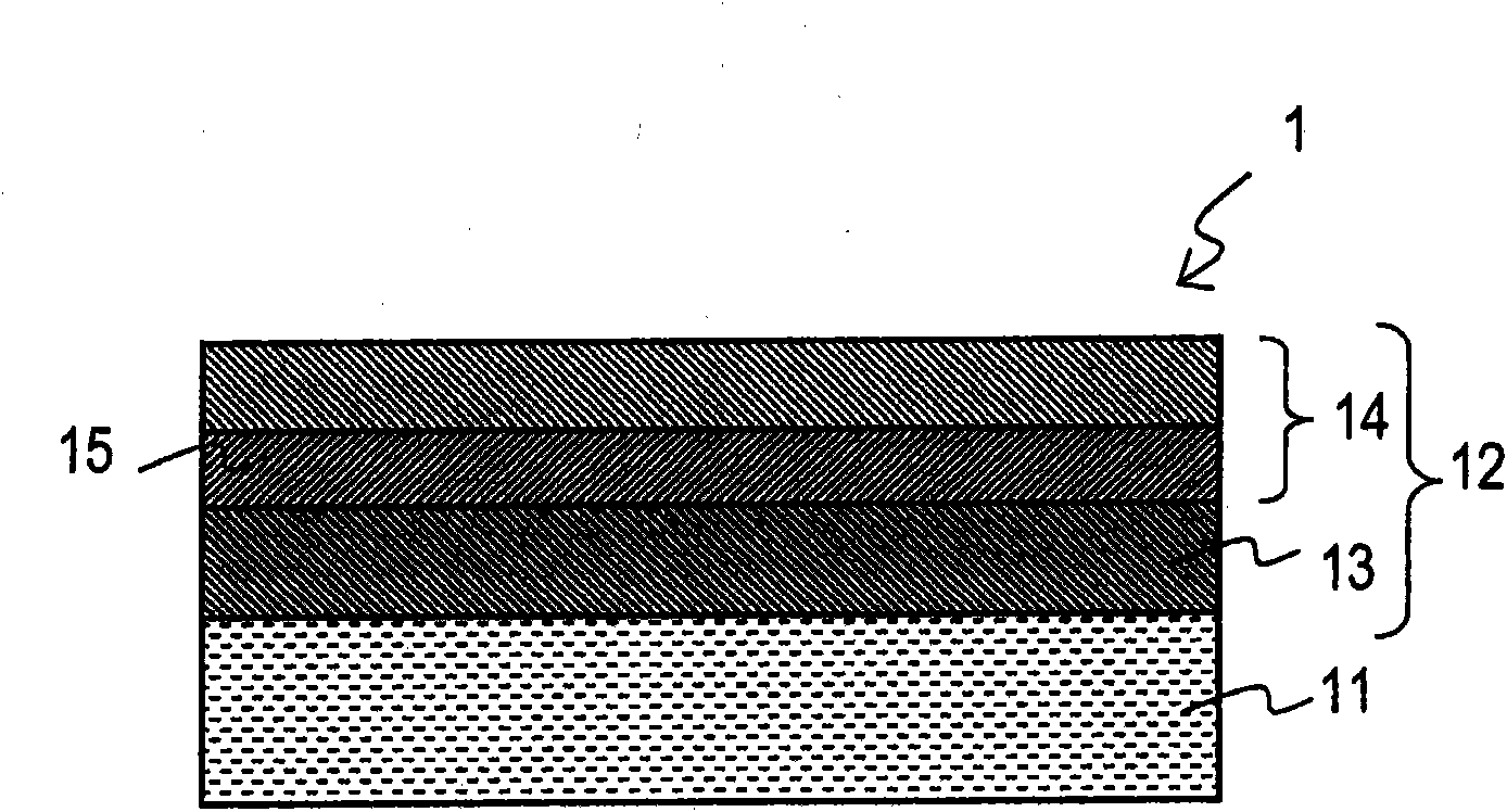
[0090] The nitride-based semiconductor light-emitting element 1 of the present embodiment is, for example, figure 1 Shown are: a selective growth layer 11 , and a nitride-based semiconductor stack structure 12 formed on the selective growth layer 11 . The selective growth layer 11 has a portion grown laterally by the ELO method.
[0091]The nitride-based semiconductor stack structure 12 includes: an active layer 13 including Al a In b Ga c N crystal layer (a+b+c=1, a≥0, b≥0, c≥0); Al d Ga e The N layer (d+e=1, d>0, e≥) 14 is located on the side opposite to the side where the selective growth layer 11 is located relative to the active layer 13 .
[0092] Al d Ga e Part of the N layer 14 has a layer (In-containing layer) 15 containing In at a concentration of 1×10 16 atms / cm 3 Above 1×10 19 atms / cm 3 The ...
Embodiment approach 2
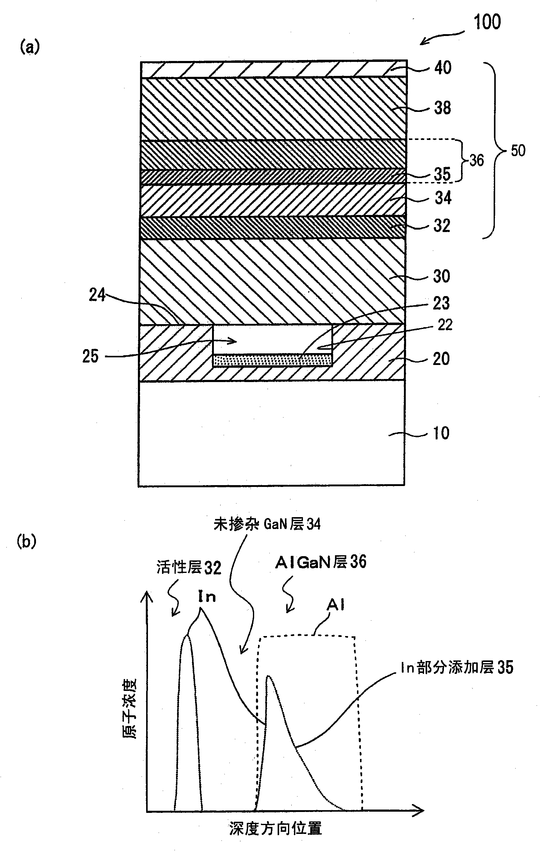
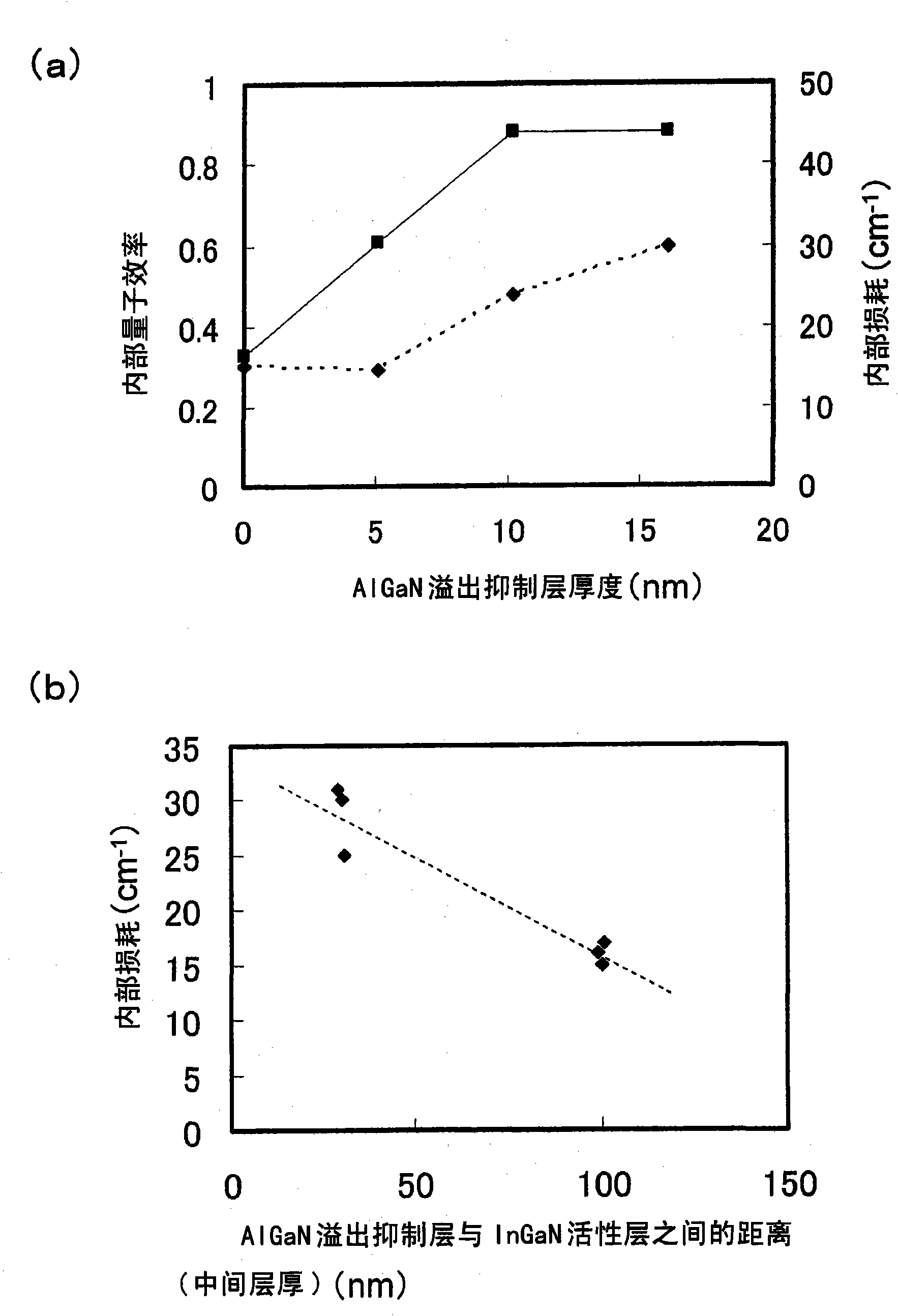
[0098] Below, refer to Figure 2 to Figure 20 A second embodiment of the nitride-based semiconductor light-emitting element according to the present invention will be described. The nitride-based semiconductor light-emitting element 100 of this embodiment is a semiconductor device using a GaN-based semiconductor, and is produced by the ELO method in order to reduce rearrangement density.
[0099] Such as figure 2 As shown in (a), the light-emitting element 100 of this embodiment has: a substrate 10; u Ga v In w N layer (u+v+w=1, u≥0, v≥0, w≥0) 20, which is formed on the substrate 10; Al x Ga y In z N crystalline layer (x+y+z=1, x≥0, y≥0, z≥0) 30, which is formed on Al u Ga v In w N layer 20 functions as a selective growth layer; semiconductor stacked structure 50, which is formed on Al x Ga y In z N crystal layer 30.
[0100] in Al u Ga v In w The N layer 20 forms a groove (recess) 22 , and a mask 23 for selective growth is formed on the bottom surface of the ...
Embodiment approach 3
[0164] Below, refer to Figure 21 A third embodiment of the nitride-based semiconductor light-emitting diode according to the present invention will be described.
[0165] The nitride-based semiconductor light-emitting element 200 of this embodiment is, for example, Figure 21 Shown are a GaN substrate 60 and a semiconductor stack 70 formed on the GaN substrate 60 .
[0166] The GaN substrate 60 of this embodiment is formed by performing the ELO method. To obtain the GaN substrate 60 , for example, a GaN layer for the GaN substrate may be formed thick while covering a part of a sapphire substrate (not shown) with a mask made of a silicon oxide film and exposing the other part. In this method, the sapphire substrate is removed after the GaN layer is formed. Alternatively, mesh-shaped titanium may be formed on a GaN layer formed on a sapphire substrate, and a GaN layer for the GaN substrate may be formed thereon. In this method, after the GaN layer is formed, titanium is use...
PUM
 Abstract
Description
Claims
Application Information