Light emitting device package structure
A technology for light-emitting components and packaging structures, applied in electrical components, semiconductor devices, circuits, etc., can solve the problems of limited application of light-emitting diodes, and achieve the effects of good light-emitting uniformity and large light-emitting area
- Summary
- Abstract
- Description
- Claims
- Application Information
AI Technical Summary
Problems solved by technology
Method used
Image

Examples
Embodiment Construction
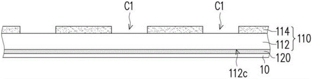
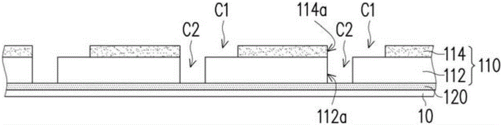
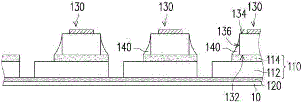
[0094] Figure 1A to Figure 1F A schematic cross-sectional view showing a manufacturing method of a light-emitting element packaging structure according to an embodiment of the present invention. It should be noted that, Figure 1A to Figure 1F It is a schematic cross-sectional view shown along one direction (such as X-X direction), so there is only one light-emitting element in each light-emitting element packaging structure formed; but in the other direction (such as Y-Y), each light-emitting element packaging structure There may also be multiple light emitting elements.
[0095] Regarding the manufacturing method of the light-emitting element packaging structure of this embodiment, first, please refer to Figure 1A , providing a wavelength conversion adhesive layer 110 , wherein the wavelength conversion adhesive layer 110 includes a low concentration adhesive layer 112 and a high concentration adhesive layer 114 . Here, the step of forming the wavelength conversion adhesi...
PUM
 Abstract
Description
Claims
Application Information
 - R&D
- Intellectual Property
- Life Sciences
- Materials
- Tech Scout
- Unparalleled Data Quality
- Higher Quality Content
- 60% Fewer Hallucinations
Browse by: Latest US Patents, China's latest patents, Technical Efficacy Thesaurus, Application Domain, Technology Topic, Popular Technical Reports.
© 2025 PatSnap. All rights reserved.Legal|Privacy policy|Modern Slavery Act Transparency Statement|Sitemap|About US| Contact US: help@patsnap.com