
Negative voltage bit line compensation circuit for sram circuit and its working method

A technology of compensation circuit and working method, applied in the field of electronics, can solve the problems of limited effect of writing ability, small negative voltage of bit line, difficult writing, etc., and achieve the effect of improving writing ability

Active Publication Date: 2020-05-26
SPREADTRUM COMM (SHANGHAI) CO LTD
View PDF3 Cites 0 Cited by
  • Summary
  • Abstract
  • Description
  • Claims
  • Application Information

AI Technical Summary

Problems solved by technology

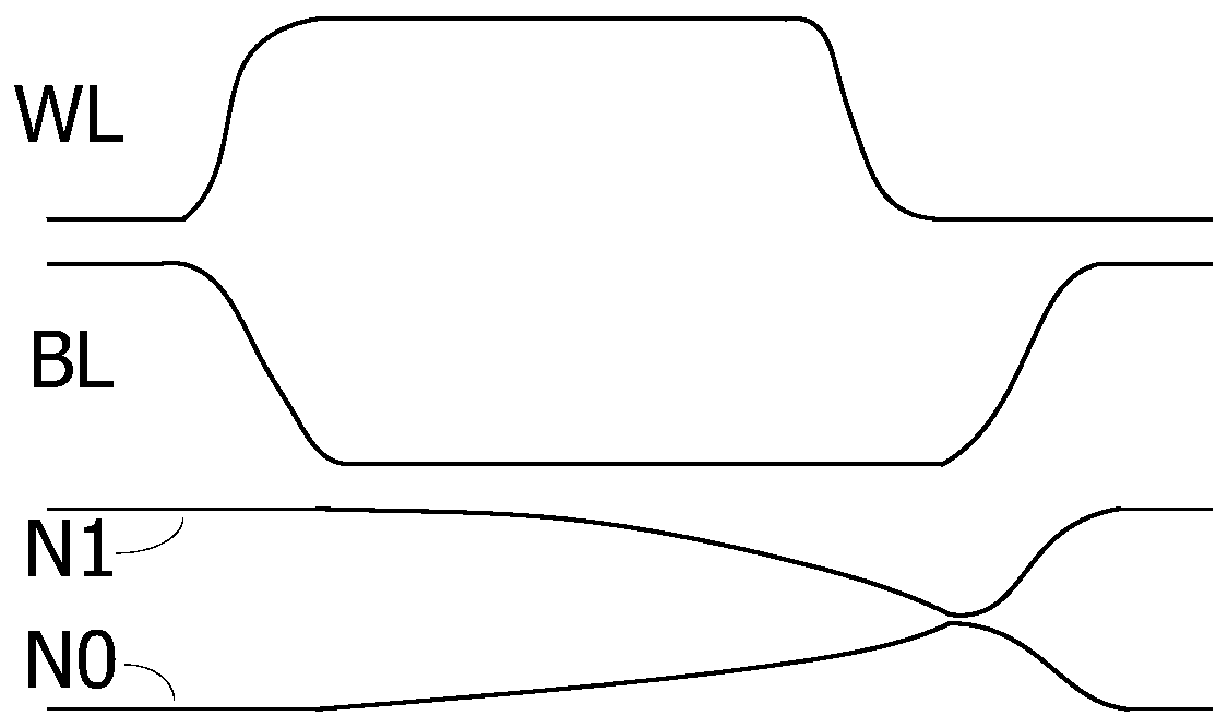
[0004] In order to solve the above problem of difficult writing, the bit line negative voltage technology was invented and applied to the design of SRAM. However, the existing bit line negative voltage technology has a small bit line negative voltage, which has limited effect on improving the writing ability.

Method used


Image

  • Negative voltage bit line compensation circuit for sram circuit and its working method
  • Negative voltage bit line compensation circuit for sram circuit and its working method
  • Negative voltage bit line compensation circuit for sram circuit and its working method

Examples


Embodiment Construction

[0058] The following will clearly and completely describe the technical solutions in the embodiments of the present invention with reference to the accompanying drawings in the embodiments of the present invention. Obviously, the described embodiments are only some, not all, embodiments of the present invention. Based on the embodiments of the present invention, all other embodiments obtained by persons of ordinary skill in the art without creative efforts fall within the protection scope of the present invention.

[0059] It should be noted that, in the case of no conflict, the embodiments of the present invention and the features in the embodiments can be combined with each other.

[0060] The present invention will be further described below in conjunction with the accompanying drawings and specific embodiments, but not as a limitation of the present invention.

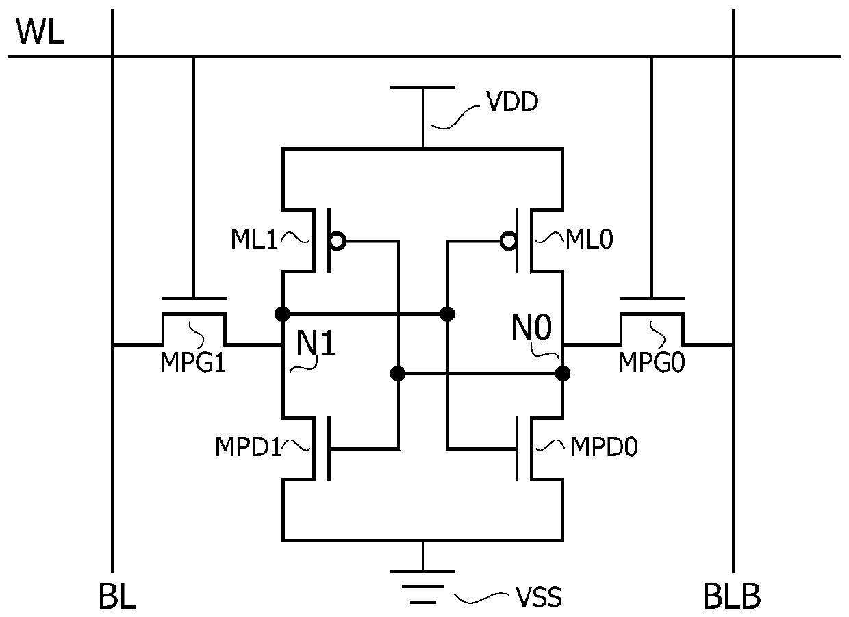
[0061] figure 1 One of the key factors affecting the write operation of the SRAM memory cell is the ratio of th...


PUM


Abstract

The invention relates to the technical field of electronics, in particular to a static random access memory (SRAM). A negative voltage bit line compensation circuit for an SRAM circuit comprises a plurality of SRAM storage units, a first auxiliary adjustment unit, a comparison unit, and a second auxiliary adjustment unit, wherein the first auxiliary adjustment unit carries out coupling on a first bit line under the action of a signal of a first write enable signal line to obtain a negative voltage, or carries out coupling on a second bit line under the action of a signal of a second write enable signal line to obtain the negative voltage; the comparison unit compares a voltage of the first bit line with a voltage of the second bit line under the action of an enable signal; and the second auxiliary adjustment unit carries out coupling on the first bit line when the voltage of the first bit line is lower than the voltage of the second bit line so as to produce a second negative voltage which is lower than the negative voltage, and carries out coupling on the second bit line when the voltage of the first bit line is higher than the voltage of the second bit line so as to produce a third negative voltage which is lower than the negative voltage. The circuit adopting the technical scheme has the advantages that the higher negative bit line voltage can be produced, so that the write capability is improved.

Description

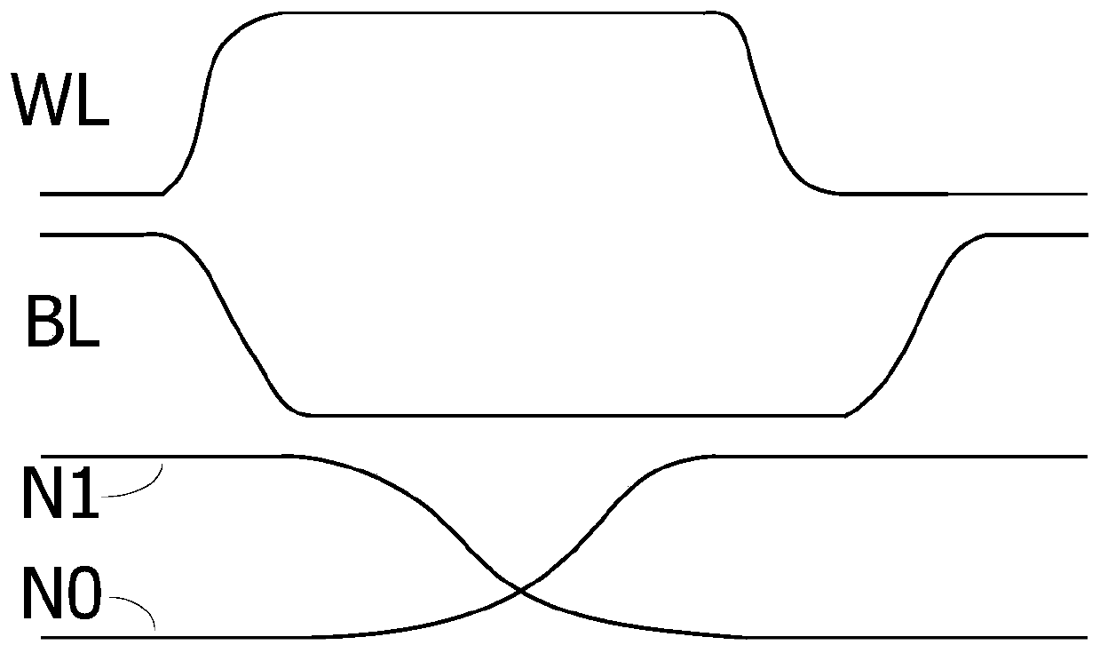
technical field [0001] The invention relates to the field of electronic technology, in particular to a static random access memory. Background technique [0002] figure 1 Shown is the most common SRAM (Static Random Access Memory) storage unit composed of six transistors. When the voltage of node N1 is high and the voltage of node N0 is low, the value stored in the storage unit is called logic 1. Otherwise it is logic 0. When it is necessary to rewrite the data stored in the SRAM storage unit, such as rewriting the stored value 1 to 0, the corresponding operation steps are: first charge the word line WL (Word Line) to a high voltage (generally equal to the power supply voltage VDD), and then The voltage of the bit line BL (Bit Line) is pulled down from the power supply voltage VDD to the ground voltage VSS, while the voltage of the bit line BLB (Bit Line Bar) is maintained at the power supply voltage VDD; since the drive capability of the PMOS transistor ML1 in the SRAM me...

Claims


Application Information

Patent Timeline
Patent Type & Authority Patents(China)
IPC IPC(8): G11C11/413G11C11/416
Inventor 不公告发明人
Owner SPREADTRUM COMM (SHANGHAI) CO LTD
Learn More