Testing structure and testing method of integrated packaged multichannel surface acoustic wave filter set
A surface acoustic wave and filter bank technology, which is applied in the direction of electronic circuit testing, instruments, measuring electronics, etc., can solve the problems of cumbersome process and inconvenient operation, and achieve the effect of high isolation, avoiding influence, and compact test structure
- Summary
- Abstract
- Description
- Claims
- Application Information
AI Technical Summary
Problems solved by technology
Method used
Image

Examples
Embodiment 1
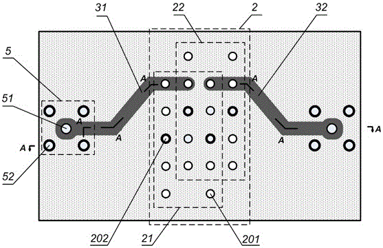
[0033] Such as Figure 1(a) , Figure 1(b) and Figure 4 As shown, the test structure for the integrated package 4-channel surface acoustic wave filter bank is:
[0034] ⑴Using FR-4 high-frequency double-sided copper-clad board to make test substrate 1, the middle part of the test substrate is the test jack area 2, and the two sides of the test jack area 2 are copper film signal wires (including the left copper film signal wire and the right copper film signal wire). film signal wires), the back of the test substrate 1 is a copper film ground plane, and the two ends of the test substrate 1 are the radio frequency connector base area 5 including the center electrode jack 51 of the radio frequency connector and the ground pin jack 52 .
[0035] (2) The test jack area includes 2 sets of jacks (the first set of jacks 21, the second set of jacks 22), each set of jacks includes a pair of grounding jacks 202 and are symmetrically distributed on the upper and lower sides of the pair ...
Embodiment 2
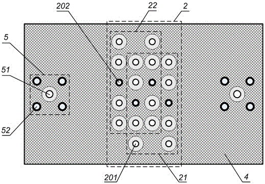
[0044] Such as Figure 2(a) , Figure 2(b) and refer to Figure 4 As shown, the test structure for integrated packaging of 6-channel surface acoustic wave filter banks (N is not a multiple of 4) is:
[0045] ⑴Using FR-4 high-frequency double-sided copper-clad board to make the test substrate 1, the middle part of the test substrate is the test socket area 2, the two sides of the test socket area are copper film signal wires, the back of the test substrate is the copper film ground plane 4, and the test substrate The two ends are the radio frequency connector base area 5 including the central electrode jack 51 and the ground pin jack 52 of the radio frequency connector.
[0046] (2) The test jack area contains 3 groups of jacks (including the first group of jacks 21, the second group of jacks 22, and the third group of jacks 23), each group of jacks includes a pair of grounding jacks 202 and are symmetrically distributed on The six signal jack pairs 201 on the upper and lowe...
Embodiment 3
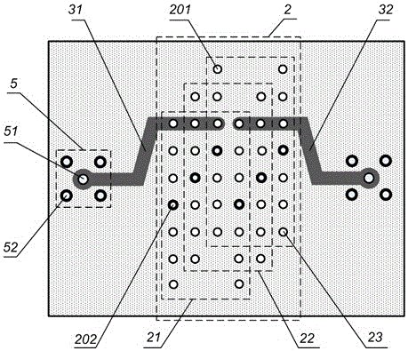
[0057] Such as Figure 3(a) , Figure 3(b) and refer to Figure 4 As shown, the specific implementation steps for integrated packaging of 8-channel surface acoustic wave filter banks (N is a multiple of 4) are:
[0058] (1) Use FR-4 high-frequency double-sided copper-clad board to make test substrate 1. The middle part of the test substrate is the test jack area 2. The two sides of the test jack area 2 are copper film signal wires. The back of test substrate 1 is the copper film ground plane. The two ends of the substrate 1 are the radio frequency connector base area 5 including the central electrode insertion hole 51 of the radio frequency connector and the ground pin insertion hole 52 .
[0059] (2) The test jack area contains 4 groups of jacks (including the first group of jacks 21, the second group of jacks 22, the third group of jacks 23, and the fourth group of jacks 24), and each group of jacks contains a grounding jack The pair of holes 202 and the eight signal jack...
PUM
 Abstract
Description
Claims
Application Information