Pixel unit and array substrate

A technology for pixel units and array substrates, applied in nonlinear optics, instruments, optics, etc., can solve the problem of pixel electrode dark lines and other problems, and achieve the effect of avoiding dark lines and electric field stability

Active Publication Date: 2017-05-10
TCL CHINA STAR OPTOELECTRONICS TECH CO LTD
View PDF4 Cites 6 Cited by
  • Summary
  • Abstract
  • Description
  • Claims
  • Application Information

AI Technical Summary

Problems solved by technology

[0004] The present invention provides a pixel unit and an array substrate to sol

Method used


Image

  • Pixel unit and array substrate
  • Pixel unit and array substrate
  • Pixel unit and array substrate

Examples


Embodiment Construction

[0020] The following will clearly and completely describe the technical solutions in the embodiments of the present invention with reference to the accompanying drawings in the embodiments of the present invention. Obviously, the described embodiments are only some, not all, embodiments of the present invention. Based on the embodiments of the present invention, all other embodiments obtained by persons of ordinary skill in the art without making creative efforts belong to the protection scope of the present invention.

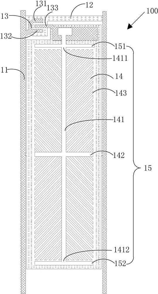
[0021] figure 1 is a schematic structural diagram of the pixel unit in the first embodiment of the present invention. Such as figure 1 As shown, the pixel unit 100 includes a data line 11 , a gate line 12 , a thin film transistor 13 , a pixel electrode 14 including at least two domains, and a shielding electrode 15 .

[0022] The TFT 13 includes a gate 131 , a source 132 and a drain 133 , the gate 131 of the TFT 13 is connected to the gate line 12 , the sour...


PUM


Abstract

The present invention discloses a pixel unit and an array substrate. The pixel unit comprises a data line, a gate line, a thin-film transistor, and a pixel electrode containing at least two domains, wherein the thin-film transistor is connected to the data line, the gate line, and the pixel electrode, respectively; and the pixel electrode further comprises at least one bucking electrode disposed parallel to the edge of the pixel electrode, with the bucking electrode being electrically connected to the pixel electrode. In such a manner, the pixel unit is able to shield interference of peripheral electric fields with the pixel electrode, allowing for more stable electrode field at the marginal area of the pixel electrode, thereby avoiding dark fringes present in the marginal area of the pixel electrode.

Description

technical field [0001] The invention relates to the field of liquid crystal display, in particular to a pixel unit and an array substrate. Background technique [0002] In the design of conventional pixel electrodes, openings are usually designed in the edge area of ​​the pixel electrodes to assist the arrangement of liquid crystals in the light-transmitting area. However, when the edge area of ​​the pixel electrode adopts an opening design, due to the existence of parasitic capacitance, the electric field generated by the metal layer close to the pixel electrode is likely to interfere with the electric field of the pixel electrode, making the potential of the pixel electrode unstable, and the pixel electrode The problem of dark lines appearing in the edge area of ​​. [0003] Wherein, the metal layer close to the pixel electrode includes a first metal layer and a second metal layer, the first metal layer is used to make gate lines, common electrode lines, etc., and the sec...

Claims


Application Information

Patent Timeline
IPC IPC(8): G02F1/1343G02F1/1362
CPCG02F1/134309G02F1/1362G02F1/136218
Inventor 邓竹明林永伦柳铭岗叶岩溪
Owner TCL CHINA STAR OPTOELECTRONICS TECH CO LTD
Why Eureka
Try Eureka