Liquid crystal display panel and manufacturing method thereof
A liquid crystal display panel and substrate technology, applied in semiconductor/solid-state device manufacturing, static indicators, optics, etc., can solve the problem of low aperture ratio of display panels
- Summary
- Abstract
- Description
- Claims
- Application Information
AI Technical Summary
Problems solved by technology
Method used
Image
Examples
Embodiment Construction
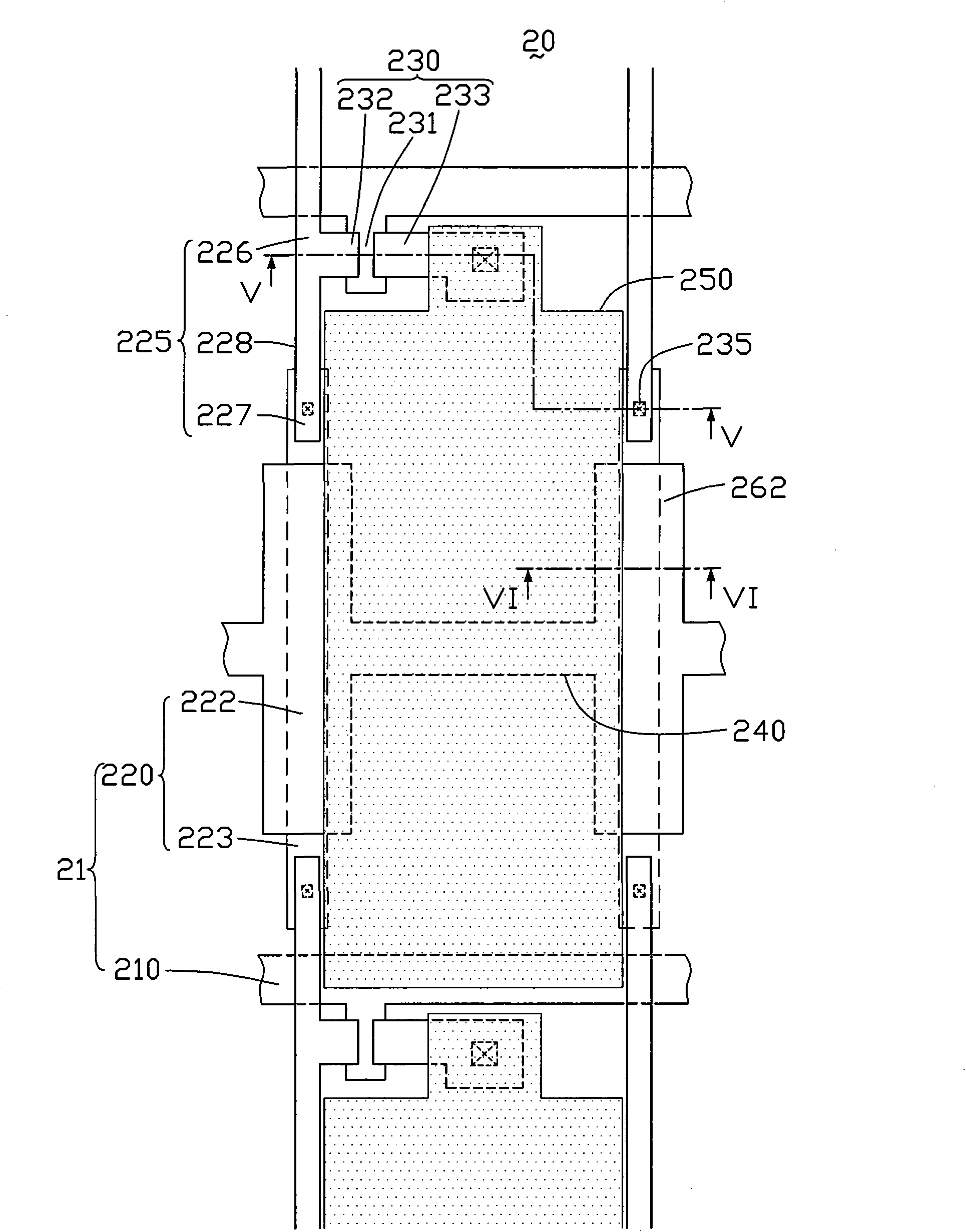
[0030] see image 3 , which is a schematic plan view of the first embodiment of the liquid crystal display panel of the present invention. The liquid crystal display panel 20 includes a plurality of signal lines 21 , a plurality of connection lines 225 , a plurality of common electrodes 262 and a plurality of common lines 240 .
[0031] The plurality of signal lines 21 includes a plurality of scan lines 210 arranged along the row direction and parallel to each other, and a plurality of data lines 220 arranged along the column direction and parallel to each other. Wherein, the scan line 210 is used to transmit scan signals, and the data line 220 is used to transmit data signals. Wherein, each data line 220 is a plurality of small segments, and two adjacent small segments of each data line 220 are respectively arranged on two sides of the scanning line 210 and do not contact the scanning line 210 .
[0032] The connection line 225 is disposed between two adjacent segments of e...
PUM
 Abstract
Description
Claims
Application Information


