Preparation method of polysilicon thin film and optoelectronic device

A technology of polysilicon thin film and amorphous silicon thin film, applied in the direction of electrical components, semiconductor devices, semiconductor/solid-state device manufacturing, etc., can solve the problems of restricting wide application, expensive equipment, MIC metal pollution, etc., achieve large-area preparation process, reduce The effect of preparation cost and saving time and cost

Active Publication Date: 2020-01-17
NINGBO INST OF MATERIALS TECH & ENG CHINESE ACADEMY OF SCI
View PDF4 Cites 0 Cited by
  • Summary
  • Abstract
  • Description
  • Claims
  • Application Information

AI Technical Summary

Problems solved by technology

However, MIC has the problem of metal contamination, which limits its wide application.
ELC uses high-power pulsed laser to irradiate the surface of amorphous silicon to reach the melting temperature in a very short time, so as to realize liquid phase recrystallization. Although it has been applied in industry, its equipment is expensive, and the repeatability of large-scale production is poor. Need to consider cost

Method used


Image

  • Preparation method of polysilicon thin film and optoelectronic device
  • Preparation method of polysilicon thin film and optoelectronic device
  • Preparation method of polysilicon thin film and optoelectronic device

Examples


preparation example Construction

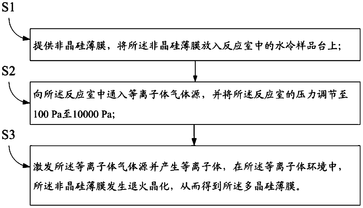
[0027] See figure 1 , The present invention provides a method for preparing a polysilicon film, which includes the following steps:

[0028] S1, providing an amorphous silicon film, and placing the amorphous silicon film on a water-cooled sample stage in the reaction chamber;

[0029] S2: Pass a plasma gas source into the reaction chamber, and control the pressure of the reaction chamber to 100 Pa to 10000 Pa;

[0030] S3. Excite the plasma gas source and generate plasma. In the plasma environment, the amorphous silicon film is annealed and crystallized, thereby obtaining the polysilicon film.

[0031] In step S1, a substrate may be further provided for supporting the amorphous silicon film. The substrate may be a silicon wafer with higher purity, or ordinary quartz glass. The amorphous silicon film may be deposited on the substrate first, and then the substrate deposited with the amorphous silicon film may be placed in the reaction chamber.

[0032] The thickness of the amorphous sil...

Embodiment 1

[0046] Deposit a 1μm thick amorphous silicon film on the cleaned 3cm×3cm silicon wafer substrate, take out the sample and install it on the water-cooled sample stage of the medium pressure plasma CVD equipment, adjust the height of the sample stage to make the surface of the substrate The distance from the plasma spray gun outlet is 30mm, close the vacuum chamber and pump the vacuum chamber to 10 -5 Pa background vacuum degree, close the gate valve connecting the molecular pump set and the cavity, open the process pump set and pressure control valve, pass in high purity Ar with a flow rate of 20slm, and adjust the pressure control valve to make the vacuum chamber The pressure reaches 800Pa, and the high purity H with a flow rate of 0.5slm 2 And turn on the radio frequency power supply to generate plasma, adjust the power of the radio frequency power supply to 14kW, the annealing temperature is 552℃, and the annealing time is 7s. Close H after annealing 2 , Turn off the plasma po...

Embodiment 2

[0048] This embodiment is basically the same as embodiment 1, except that the substrate is a quartz glass substrate, and the plasma gas sources are Ar and H 2 The flow rate of the plasma gas source is 10slm, the cavity pressure of the reaction chamber is 200Pa, the annealing power is 16kW, the annealing time is 5s, and the annealing temperature is 600°C.


PUM

PropertyMeasurementUnit
thicknessaaaaaaaaaa
thicknessaaaaaaaaaa
poweraaaaaaaaaa

Abstract

The present invention provides a preparation method of a polycrystalline silicon film. The preparation method comprises a first step of providing an amorphous silicon film, and putting the amorphous silicon film on a water cooling sample table in a reaction room; a second step of inletting a plasma gas source into the reaction room, and adjusting the pressure of the reaction room to 100Pa-10000Pa; and a third step of stimulating the plasma gas source and generating plasma, annealing and crystallizing the amorphous silicon film in the plasma environment so as to obtain the polycrystalline silicon film. According to the preparation method, the amorphous silicon film is put in a radio frequency plasma environment generated through inductive coupling under medium pressure, so that the amorphous silicon film is annealed and crystalized rapidly to prepare the polycrystalline silicon film rapidly at low temperature. In the preparation method, common glass and other cheap substrates are used, so that the preparation costs are greatly reduced, further the time costs are greatly saved, and the method has the advantages of low cost, mass production and simple technology.

Description

Technical field [0001] The invention relates to the field of semiconductors, and in particular to a method for preparing a polysilicon film and a photoelectric device using the polysilicon film. Background technique [0002] Polysilicon thin films have received widespread attention due to their good properties. In the field of large-array liquid crystal displays, large-grain polycrystalline silicon films have high mobility similar to monocrystalline silicon films, and can be used for the preparation of large-area, fast-response field effect transistors, sensors and other optoelectronic devices. In terms of solar cells, polycrystalline silicon films are not only sensitive to long-wavelength light, but also have a high absorption coefficient for visible light; they have the same stability as crystalline silicon, and will not produce severe light-induced attenuation effects similar to amorphous silicon. [0003] The existing polysilicon thin film preparation processes mainly include ...

Claims


Application Information

Patent Timeline
Patent Type & Authority Patents(China)
IPC IPC(8): H01L21/02H01L31/0216
CPCH01L21/02667H01L21/02689H01L31/0216
Inventor 芦子玉邬苏东叶继春高平奇丁丽
Owner NINGBO INST OF MATERIALS TECH & ENG CHINESE ACADEMY OF SCI
Why Eureka
Try Eureka