Organic light-emitting diode display

A technology of organic light-emitting elements and displays, applied in the direction of diodes, organic semiconductor devices, electric solid-state devices, etc., can solve problems such as efficiency reduction and color shift, and achieve the effects of reducing color shift and improving color reproducibility

Active Publication Date: 2017-05-10
SAMSUNG DISPLAY CO LTD
View PDF25 Cites 26 Cited by
  • Summary
  • Abstract
  • Description
  • Claims
  • Application Information

AI Technical Summary

Problems solved by technology

However, since the light generated from the organic emission layer is partially or completely reflected between the organic emission layer and one of the electrodes, the efficiency of light transmission to the environment is reduced.
[0006] In addition, there may be a color shift caused by changing color shading (hue) according to the angle between the observer and the monitor

Method used


Image

  • Organic light-emitting diode display
  • Organic light-emitting diode display
  • Organic light-emitting diode display

Examples


Embodiment Construction

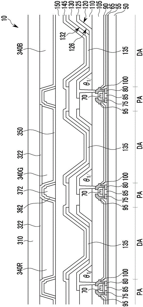
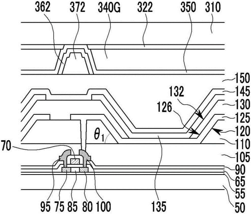
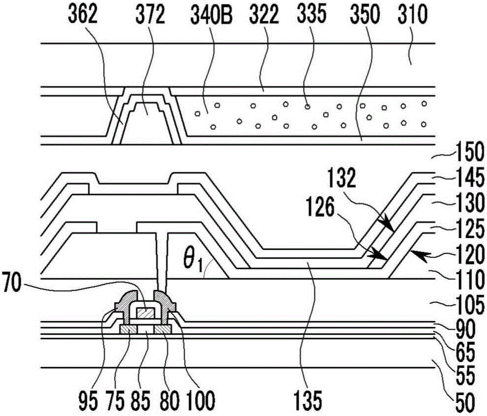
[0050] Hereinafter, embodiments will be described more fully with reference to the accompanying drawings. As those skilled in the art would realize, the described embodiments may be modified in various different ways, all without departing from the spirit or scope of the present disclosure.

[0051] To clearly describe the present disclosure, parts irrelevant to the description will be omitted, and the same reference numerals will refer to the same elements throughout the specification.

[0052] In addition, in the drawings, the size and thickness of each element are arbitrarily shown for convenience of description, and the present disclosure is not necessarily limited to those shown in the drawings. In the drawings, the thickness of layers, films, panels, regions, etc., are exaggerated for clarity. In the drawings, the thicknesses of some layers and regions are exaggerated for convenience of description.

[0053] In this disclosure, the term "substantially" includes meaning...


PUM


Abstract

Disclosed is an organic light-emitting diode (OLED) display. In one aspect, the OLED display includes a first substrate, an insulating layer arranged above the first substrate and including a first inclined part, and a first electrode arranged on the insulating layer. The OLED display also includes a luminous element layer arranged on the first electrode, a second electrode arranged on the luminous element layer, and color conversion layers and a transmission layer which are arranged on the second electrode. The first electrode includes a second inclined part, and the second inclined part is arranged on the first inclined part of the insulating layer and is inclined along the first inclined part of the insulating layer.

Description

[0001] Cross References to Related Applications [0002] This application claims priority and benefit from Korean Patent Application No. 10-2015-0152548 filed with the Korean Intellectual Property Office on October 30, 2015, the entire contents of which are incorporated herein by reference. technical field [0003] The described technology generally relates to organic light emitting diode (OLED) displays. Background technique [0004] An OLED display includes an organic light emitting element including a hole injection electrode, an organic emission layer, and an electron injection electrode. Each organic light-emitting element emits light using energy generated when excitons generated by combining electrons and holes transition from an excited state to a ground state within the organic emission layer, and using this light emission, pixels (including OLEDs) The combination can display a predetermined image. [0005] OLED displays generally have a structure in which an anod...

Claims


Application Information

Patent Timeline
Patent Type & Authority Applications(China)
IPC IPC(8): H01L27/32H01L51/52
CPCH10K59/38H10K59/122H10K50/805H10K50/856H10K50/813H10K50/818H10K50/841H10K50/854H10K50/19H10K50/865H10K2102/331H10K59/123H10K59/124H10K2102/3026
Inventor 李栢熙南敏基朴海日
Owner SAMSUNG DISPLAY CO LTD
Why Eureka
Try Eureka