
SMD type oled display unit device, display screen and manufacturing method thereof

A display unit, chip-type technology, applied in the field of OLED display, can solve the problems of large-area driving backplane yield reduction, large-size display production yield reduction, process management difficulties, etc., to achieve yield improvement, simple driving, The effect of reducing the difficulty of process management

Active Publication Date: 2020-02-07
齐鹏
View PDF8 Cites 0 Cited by
  • Summary
  • Abstract
  • Description
  • Claims
  • Application Information

AI Technical Summary

Problems solved by technology

[0003] Since the OLED display is a current-type display device, the control of the luminous brightness of the display device is determined by the current density passing through the device, and in the existing manufacturing process, the positive and negative electrodes need to be arranged on the upper and lower sides of the OLED material, which requires the drive circuit to be very complex, which will lead to a decrease in the yield of the large-area drive backplane, and the process management in EL production is also extremely difficult, which will easily lead to a further decrease in the production yield of large-size displays, or even make it impossible to apply
In addition, due to the stability of the process, the unique environmental sensitivity of the OLED display device process, and the unique life of the OLED display device, even if a perfect display screen can be produced in the OLED large-area display, after a period of use , dead spots (not displayed), dark spots, and short-circuit spots still occur frequently, because in the existing manufacturing process, several OLED display units are directly integrated with the positive and negative electrode drive boards, and it is impossible to conveniently and effectively detect individual defects. Repair, can only replace the new screen, the price is extremely expensive

Method used


Image

  • SMD type oled display unit device, display screen and manufacturing method thereof
  • SMD type oled display unit device, display screen and manufacturing method thereof
  • SMD type oled display unit device, display screen and manufacturing method thereof

Examples


Embodiment Construction

[0053] In order to make the technical problems, technical solutions and advantages to be solved by the present invention clearer, the following will describe in detail with reference to the drawings and specific embodiments.

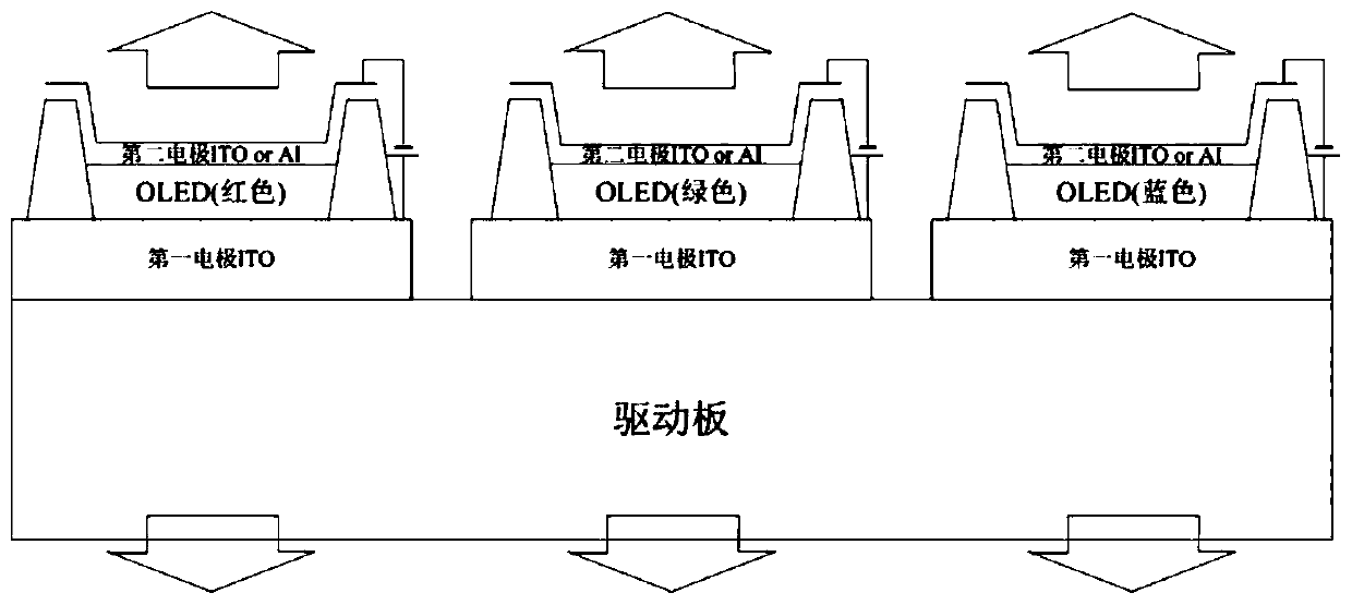
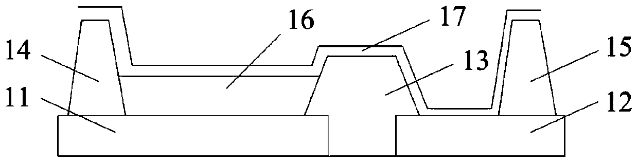
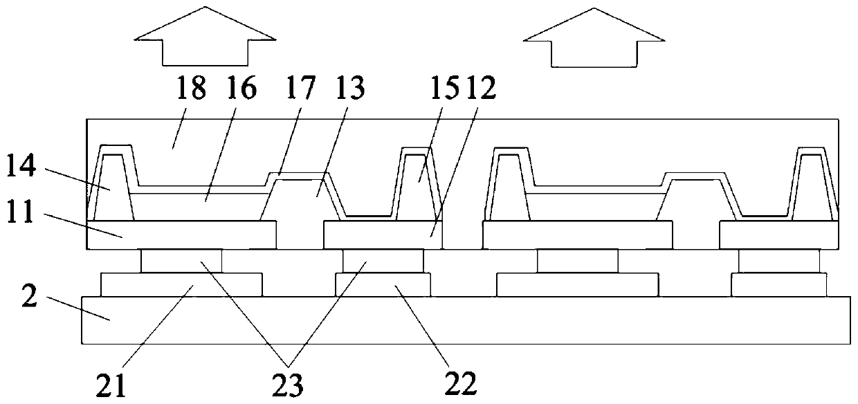
[0054] On the one hand, the present invention provides a patch type OLED display unit device, such as figure 2 As shown, it includes a first electrode 11 and a second electrode 12 arranged side by side, an insulating layer 13 is arranged between the first electrode 11 and the second electrode 12, and an insulating layer 13 is arranged on the edges of the first electrode 11 and the second electrode 12 respectively. Layer 13 constitutes a first edge layer 14 and a second edge layer 15 of the channel structure;

[0055] The groove structure formed by the first edge layer 14 and the insulating layer 13 is provided with an OLED luminescent material 16 connected to the upper surface of the first electrode 11, and the upper surface of the OLED luminescent mate...


PUM

PropertyMeasurementUnit
thicknessaaaaaaaaaa
thicknessaaaaaaaaaa
thicknessaaaaaaaaaa

Abstract

The invention discloses a chip-type OLED display unit device, a display screen and a manufacturing method thereof, belonging to the field of OLED displays. The chip-type OLED display unit device includes a first electrode and a second electrode arranged side by side, and the first electrode An insulating layer is arranged between the first electrode and the second electrode, and the edges of the first electrode and the second electrode are respectively provided with a first edge layer and a second edge layer forming a groove structure with the insulating layer. The groove structure formed by the first edge layer and the insulating layer is provided with an OLED light-emitting material connected to the upper surface of the first electrode, and the upper surface of the OLED light-emitting material is provided with a layer passing through the surface of the insulating layer. an electrode connection layer connected to the second electrode. Compared with the prior art, the present invention has the characteristics of simple driving, improved yield, simple repair, convenient operation, reduced use cost, and extended service life of large-area OLED displays.

Description

technical field [0001] The invention relates to the field of OLED display, in particular to a chip-type OLED display unit device, a display screen and a manufacturing method thereof. Background technique [0002] The OLED display is composed of a number of light-emitting pixels and a driver board that drives the light-emitting pixels to emit light. Each pixel is an OLED display device. Among them, the OLED display device can be composed of red, green and blue (three primary colors) three light-emitting OLED materials. A full-color display device, the upper and lower sides of the three light-emitting OLED materials are provided with positive and negative electrodes corresponding to each light-emitting OLED material, and different voltages are applied to the positive and negative electrodes of the three light-emitting OLED materials, and the generated currents are respectively After flowing through the three OLED light-emitting materials, the three light-emitting OLED material...

Claims


Application Information

Patent Timeline
Patent Type & Authority Patents(China)
IPC IPC(8): H01L27/32H01L51/52H01L51/56
CPCH10K59/12H10K50/805H10K2102/301H10K71/00
Inventor 齐鹏
Owner 齐鹏
Features
  • Generate Ideas
  • Intellectual Property
  • Life Sciences
  • Materials
  • Tech Scout
  • Unparalleled Data Quality
  • Higher Quality Content
  • 60% Fewer Hallucinations
Learn More