Photosensitive assembly, fingerprint recognition panel and apparatus

A photosensitive component and fingerprint recognition technology, applied in the photosensitive field, can solve problems such as noise interference

Active Publication Date: 2017-05-17
BOE TECH GRP CO LTD
View PDF6 Cites 40 Cited by
  • Summary
  • Abstract
  • Description
  • Claims
  • Application Information

AI Technical Summary

Problems solved by technology

[0005] Embodiments of the present invention provide a photosensitive component, a fingerprint identification panel and a device, which can solve the problem of noise interference caused by light directly incident on the photosensitive device from the side

Method used


Image

  • Photosensitive assembly, fingerprint recognition panel and apparatus
  • Photosensitive assembly, fingerprint recognition panel and apparatus
  • Photosensitive assembly, fingerprint recognition panel and apparatus

Examples


Embodiment 1

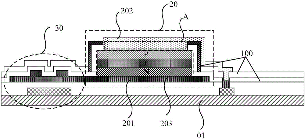
[0043] Such as image 3 As shown, the isolation dielectric layer 100 includes a first insulating layer 101 , a second insulating layer 102 and a light shielding portion 200 .

[0044] Wherein, the first insulating layer 101 is located between the first electrode 201 and the PIN semiconductor layer 203, the PIN semiconductor layer 203 is connected to the first electrode 201 through a via hole located on the first insulating layer 101, and the first insulating layer 101 covers at least The thin film transistor 30 and the first electrode 201 are not in contact with the part of the PIN semiconductor layer 203 .

[0045] The second insulating layer 102 is located between the first transparent conductive pattern 2021 and the second transparent conductive pattern 2022, the second insulating layer 102 at least covers the side of the PIN semiconductor layer 203 that is not in contact with the first insulating layer 101, and is insulated from the first The layer 101 is in contact, that...

Embodiment 2

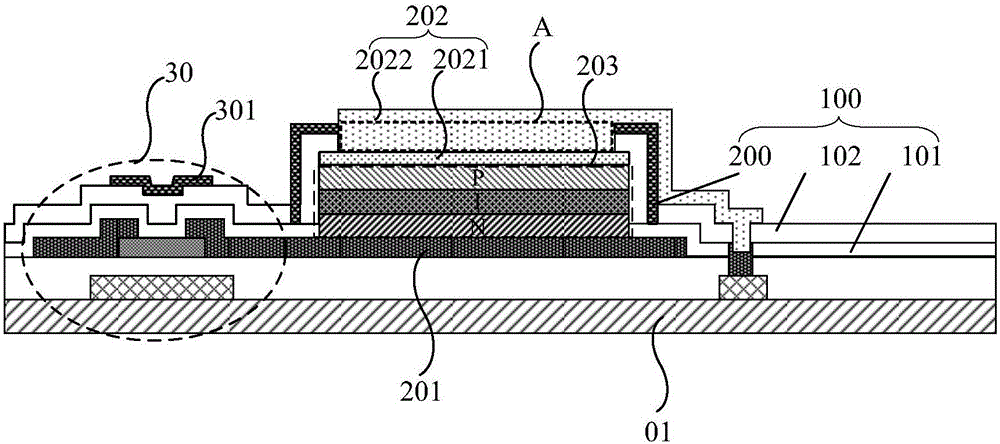
[0056] Such as Figure 5 As shown, the isolation dielectric layer 100 includes a first insulating layer 101 and a light shielding portion 200 .

[0057] Wherein, the first insulating layer 101 is located between the first transparent conductive pattern 2021 and the second transparent conductive pattern 2022; the first insulating layer 101 at least covers the thin film transistor 30, the part of the first electrode 201 that is not in contact with the PIN semiconductor layer 203 and side of the PIN semiconductor layer 203 .

[0058] The light shielding portion 200 is located between the first insulating layer 101 and the second transparent conductive pattern 2022 , and the light shielding portion 200 is disposed on the side of the PIN semiconductor layer 203 . In this way, the light can only be incident on the PIN semiconductor layer through the second electrode after being reflected by the finger, and cannot directly pass through the light-shielding portion on the side of the ...

Embodiment 3

[0068] Such as Figure 7 As shown, the isolation dielectric layer 100 includes a first insulating layer 101 and a light shielding portion 200 .

[0069] The first insulating layer 101 is located between the first electrode 101 and the PIN semiconductor layer 203, and the PIN semiconductor layer 203 is connected to the first electrode 101 through a via hole located on the first insulating layer 101; the first insulating layer 101 at least covers the thin film transistor 30 and the portion of the first electrode 101 not in contact with the PIN semiconductor layer 203 .

[0070] The light-shielding part 200 is mainly made of black insulating material, and is located between the first transparent conductive pattern 2021 and the second transparent conductive pattern 2022. The light-shielding part 200 covers at least the side of the PIN semiconductor layer 203, and the second transparent conductive pattern 2022 passes through the light-shielding part. The via hole A on 200 is conne...


PUM


Abstract

Embodiments of the invention provide a photosensitive assembly, and a fingerprint recognition panel and apparatus, relate to the photosensitive technical field, and can solve the problem of noise interference caused by direct incidence of light rays from a side surface to a photosensitive device. The photosensitive assembly comprises a thin film transistor and a photosensitive device arranged on a substrate, wherein the photosensitive device comprises a first electrode, a PIN semiconductor layer and a second electrode which are arranged in sequence in a direction far from the substrate; the first electrode is connected with the drain of the thin film transistor; the first electrode is a non-transparent electrode; the second electrode is a transparent electrode; the photosensitive assembly also comprises an isolation dielectric layer which covers the thin film transistor, the part, not in contact with the PIN semiconductor layer, of the first electrode, and the side surface of the PIN semiconductor layer; the upper surface of the isolation dielectric layer is in contact with the second electrode; the isolation dielectric layer is used for insulating and isolating the second electrode from the first electrode, the side surface of the PIN semiconductor layer and the thin film transistor; and the isolation dielectric layer comprises a light shading part arranged on the side surface of the PIN semiconductor layer.

Description

technical field [0001] The invention relates to the field of photosensitive technology, in particular to a photosensitive component, a fingerprint identification panel and a device. Background technique [0002] Photosensitive devices can convert light of different intensities into photocurrents of different sizes, so photosensitive elements are widely used in the fields of obtaining light intensity parameters and obtaining patterns through different light intensities. [0003] For example, in the field of fingerprint identification components to acquire and identify fingerprints, such as figure 1 As shown, when the finger is placed above the photosensitive device 20 in the fingerprint recognition element, the light emitted by the light source 10 located below the photosensitive device 20 can pass through the fingerprint recognition element, and enter the valleys and ridges of the finger, and pass through the fingerprint recognition element. Reflection is incident on the ph...

Claims


Application Information

Patent Timeline
Patent Type & Authority Applications(China)
IPC IPC(8): H01L31/105G06K9/00
CPCH01L31/105G06V40/1318
Inventor 刘英明董学吕敬王海生陈小川丁小梁许睿贾亚楠赵利军李昌峰郭玉珍
Owner BOE TECH GRP CO LTD
Why Eureka
Try Eureka