

Circuit for transistor level implementation scheme of five input end combination logical circuit
A combinational logic, five-input technology, applied in logic circuits, logic circuits with logic functions, electrical components, etc., can solve the problems of large transmission delay, large signal transmission delay, large silicon chip area, etc., to reduce the number of transistors, The effect of wafer area reduction
- Summary
- Abstract
- Description
- Claims
- Application Information
AI Technical Summary
Problems solved by technology
Method used
Image

Examples
Embodiment Construction
[0016] The preferred embodiments of the present invention are given below in conjunction with the accompanying drawings to describe the technical solution of the present invention in detail.
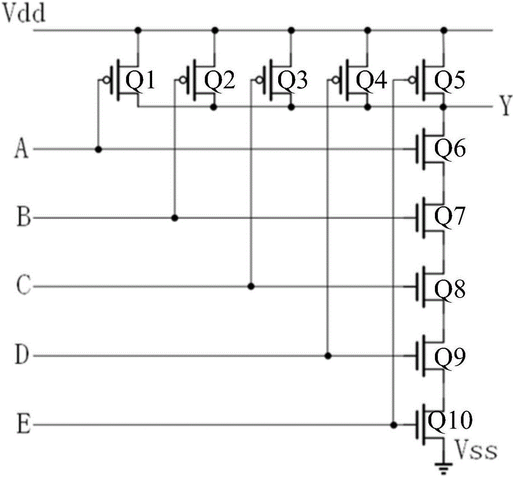
[0017] Such as figure 1 As shown, the five-input combinational logic circuit of the present invention includes a first transistor Q1, a second transistor Q2, a third transistor Q3, a fourth transistor Q4, a fifth transistor Q5, and a sixth transistor Q5. Transistor Q6, seventh triode Q7, eighth triode Q8, ninth triode Q9, thirteenth triode Q10, the drain of the first triode Q1, the drain of the second triode Q2, The drain of the third triode Q3, the drain of the fourth triode Q4 and the drain of the fifth triode Q5 are connected, the source of the first triode Q1, the source of the second triode Q2 pole, the source of the third transistor Q3, the source of the fourth transistor Q4 and the source of the fifth transistor Q5 are connected, the gate of the first transistor Q1 is connected ...
PUM
 Abstract
Description
Claims
Application Information