Supercharge Your Innovation With Domain-Expert AI Agents!

An LCD array substrate, LCD panel and LCD pixel circuit

A technology for array substrates and pixel circuits, applied in instruments, static indicators, nonlinear optics, etc., can solve problems affecting display quality and achieve the effects of reducing the risk of afterimages, increasing capacitance, and reducing feedthrough voltage

Active Publication Date: 2019-02-26
TCL CHINA STAR OPTOELECTRONICS TECH CO LTD
View PDF6 Cites 0 Cited by
  • Summary
  • Abstract
  • Description
  • Claims
  • Application Information

AI Technical Summary

Problems solved by technology

[0005] The purpose of the present invention is to provide an LCD array substrate, LCD panel and LCD pixel circuit, aiming to solve the problem in the prior art that the feed-through voltage affects the display quality

Method used


Image

  • An LCD array substrate, LCD panel and LCD pixel circuit
  • An LCD array substrate, LCD panel and LCD pixel circuit
  • An LCD array substrate, LCD panel and LCD pixel circuit

Examples


Embodiment Construction

[0021] The following descriptions of the various embodiments refer to the accompanying drawings to illustrate specific embodiments in which the present invention can be practiced. The directional terms mentioned in the present invention, such as "up", "down", "front", "back", "left", "right", "inside", "outside", "side", etc., are for reference only The orientation of the attached schema. Therefore, the directional terms used are used to illustrate and understand the present invention, but not to limit the present invention.

[0022] In the figures, blocks with similar structures are denoted by the same reference numerals.

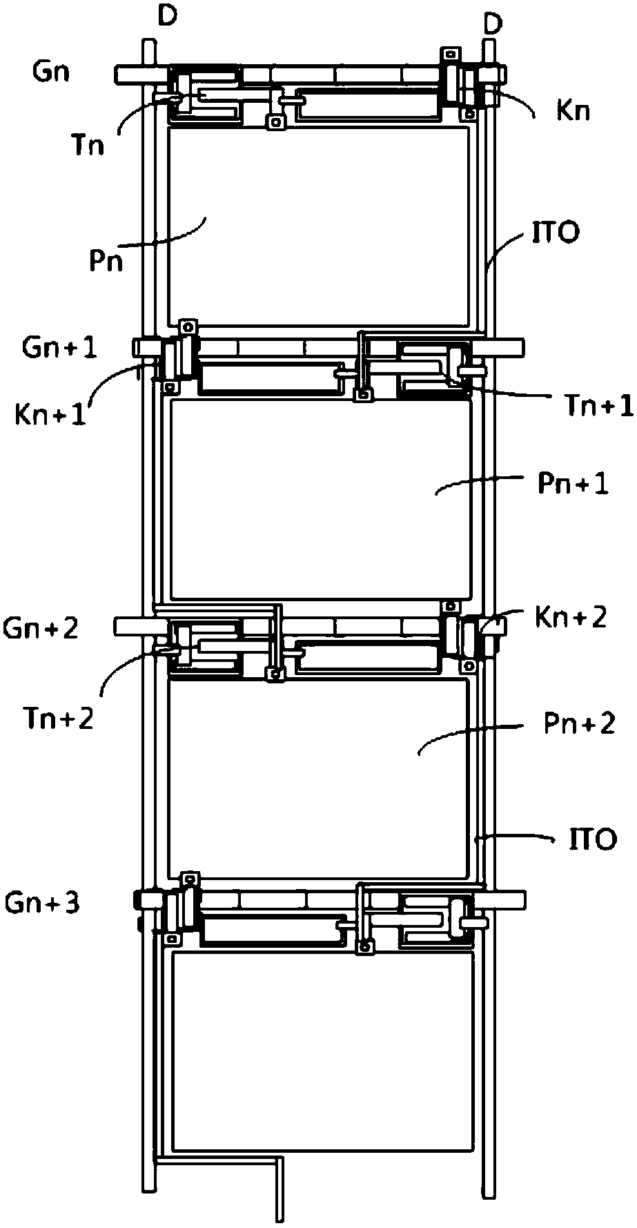
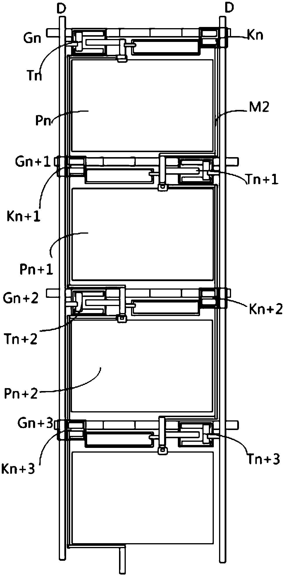
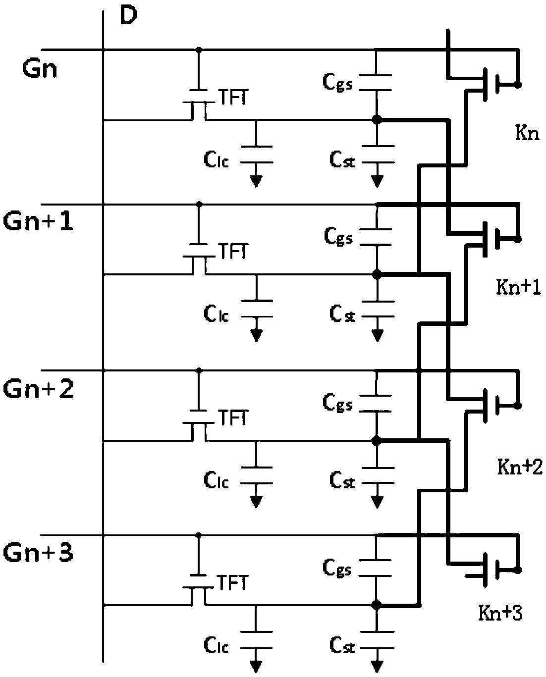
[0023] Please refer to figure 1 , is a plan view of the array substrate of a preferred embodiment of the LCD array substrate of the present invention, and the LCD array substrate includes: a substrate (not shown in the figure), a plurality of gate lines formed on the substrate (using Gn, Gn+1 . +1 to indicate), a pixel electrode P is formed in each pix...


PUM


Abstract

The invention discloses an LCD array substrate, an LCD panel and an LCD pixel circuit. The LCD array substrate includes: a substrate, a plurality of gate lines and data lines formed on the substrate, and the gate lines cross the data lines. A plurality of pixel units are formed, and a pixel electrode is formed in each pixel unit. The first thin film transistor also includes a connection switch controlled by a gate line, and the connection switch is controlled to be turned on, so that the pixel units located in the same column , the electrical connection between the pixel electrodes of the pixel units in the upper row and the pixel electrodes in the same column and the lower row of pixel units. In the present invention, by adding a connection switch for each pixel unit, the pixel electrodes of the previous row of the current row of pixel units are connected with the pixel electrodes of the next row to increase the capacitance, thereby reducing the feed-through voltage and reducing the risk of afterimages.

Description

technical field [0001] The invention relates to the field of liquid crystal display, in particular to an LCD array substrate, an LCD panel and an LCD pixel circuit. Background technique [0002] LCD (Liquid Crystal Display, liquid crystal display) uses the change of the electric field strength clamped on the liquid crystal molecules to change the orientation of the liquid crystal molecules to control the intensity of light transmission to display images. Currently, liquid crystal displays have been widely used in various terminal display devices of large, medium and small sizes due to their characteristics of light weight, small volume, and thin thickness. The LCD is mainly composed of an array substrate and a color filter substrate in the box. The array substrate is formed with gate lines, data lines, pixel electrodes and thin film transistors. Each pixel electrode is controlled by a thin film transistor. When the thin film transistor is turned on, the pixel electrode is in...

Claims


Application Information

Patent Timeline
Patent Type & Authority Patents(China)
IPC IPC(8): G02F1/1362G02F1/1368G02F1/133
CPCG02F1/13306G02F1/136213G02F1/136286G02F1/1368G02F1/13624G09G2320/0219G09G2310/0248G09G2310/0251G09G3/3614G02F1/133514G02F2201/123G02F1/136295G02F1/133397
Inventor 安立扬
Owner TCL CHINA STAR OPTOELECTRONICS TECH CO LTD
Features
  • R&D
  • Intellectual Property
  • Life Sciences
  • Materials
  • Tech Scout
  • Unparalleled Data Quality
  • Higher Quality Content
  • 60% Fewer Hallucinations
Learn More