
Substrate etching method

A substrate and main etching technology, which is applied in the manufacture of electrical components, circuits, semiconductor/solid-state devices, etc., can solve the problems of reducing the bottom width of the substrate pattern, reducing the production efficiency, and failing to achieve it, so as to increase the bottom of the pattern. The effect of width, increasing remaining thickness, bottom width and height is satisfied

Active Publication Date: 2020-07-17
BEIJING NAURA MICROELECTRONICS EQUIP CO LTD
View PDF6 Cites 0 Cited by
  • Summary
  • Abstract
  • Description
  • Claims
  • Application Information

AI Technical Summary

Problems solved by technology

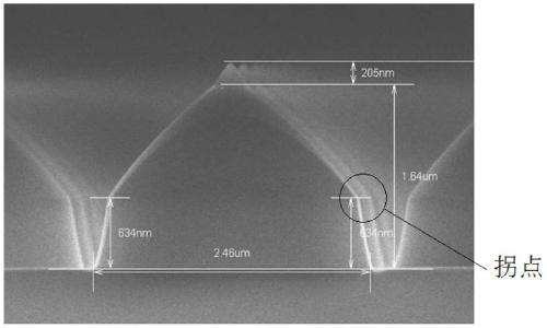
However, reducing the etching rate will not only lead to longer process time, thereby reducing production efficiency, but also because the corner height formed on the pattern sidewall during the process is too high, resulting in that the corner cannot be eliminated after the process ,like figure 1 Shown is the scanning electron microscope image of the substrate pattern morphology obtained by using a lower etching rate
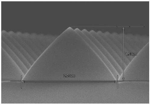
[0005] Another existing adjustment method is to reduce the temperature of the substrate by using a higher back-blowing air pressure during the process, so as to reduce the volatilization of by-products and make them adhere to the sidewall, thereby increasing the bottom of the substrate pattern. Wide, but because lowering the substrate temperature will increase the etching rate of the photoresist, resulting in a lower height of the substrate pattern, such as figure 2 Shown is the scanning electron microscope image of the substrate pattern morphology obtained by using a higher back blowing pressure during the whole process, by figure 2 It can be seen that although the bottom width of the pattern is 2.75 μm, which meets the requirements, the height of the pattern is only 1.53 μm, which does not meet the required range (such as 1.6-1.7 μm)
Conversely, if the substrate temperature is increased, although the height of the substrate pattern can be increased, the bottom width of the substrate pattern will be reduced

Method used


Image

  • Substrate etching method
  • Substrate etching method
  • Substrate etching method

Examples


specific Embodiment

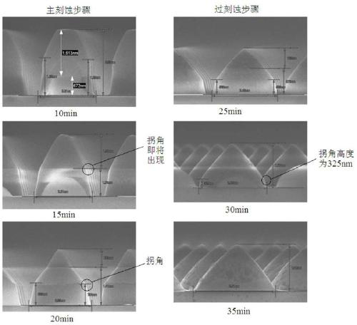
[0046] The following is a specific embodiment of the substrate etching method provided by the present invention, the substrate etching method specifically includes the following steps:

[0047] The main etching step, which further comprises step ME1 and step ME2, wherein,

[0048] The process parameters of step ME1 are: the chamber pressure of the reaction chamber is 2.5mT; the power of the upper electrode is 1400W; the power of the lower electrode is 350W; the flow rate of the etching gas is 80sccm; the process time is 18min;

[0049] The process parameters of step ME2 are: the chamber pressure of the reaction chamber is 2.5mT; the power of the upper electrode is 1400W; the power of the lower electrode is 350W; the etching gas is 80sccm; the process time is 7min;

[0050] Overetching step, which further includes step OE1 and step OE2, wherein,

[0051] The process parameters of step OE1 are: the chamber pressure of the reaction chamber is 2.2mT; the power of the upper electr...


PUM


Abstract

The invention provides a substrate etching method comprising a main etching step and an over etching step. The main etching step further comprises a step S1 and a step S2. When a corner appears in a graph sidewall, the step S1 is ended and the step S2 is simultaneously started. The over etching step comprises a step S3 and a step S4. When the height of the corner reaches the fixed value, the step S3 is ended and the step S4 is simultaneously started. The back blowing air pressure adopted for cooling a substrate in the step S1 and the step S4 is less than the back blowing air pressure adopted for cooling the substrate in the step S2 and the step S3. According to the substrate etching method, the bottom width of the substrate graph can be increased under the condition of having low influence on the height of the substrate graph so as to obtain the substrate graph of which the bottom width and the height meet the requirements.

Description

technical field [0001] The invention relates to the field of semiconductor manufacturing, in particular to a substrate etching method. Background technique [0002] A patterned sapphire substrate (Patterned Sapphire Substrate, PSS for short), as a commonly used method to improve the light extraction efficiency of GaN-based LED devices, has been widely used in the field of LED preparation. Appropriate pattern shape and size are necessary conditions for reducing epitaxial crystal defects and improving internal quantum efficiency. At present, the ideal substrate pattern is a conical structure with a height of 1-2 μm, an interval of 2-3 μm, and a bottom width of 2-3 μm. 3μm, the sidewall bevel angle is 31.6°. [0003] ICP (Inductively Coupled Plasma, Inductively Coupled Plasma) technology is a method for preparing sapphire pattern substrates, which is widely used for its advantages of being able to control plasma density and bombardment energy, and being suitable for automatic ...

Claims


Application Information

Patent Timeline
Patent Type & Authority Patents(China)
IPC IPC(8): H01L21/3065
CPCH01L21/3065
Inventor 朱印伍吴鑫
Owner BEIJING NAURA MICROELECTRONICS EQUIP CO LTD
Learn More