Magnetic tunneling junction configuration and a method for making the same

a tunnel junction and magnetic tunneling technology, applied in the field of magnetic tunneling junction configuration and a manufacturing method, can solve the problem that the method may be substantially absent of oxygen plasma, and achieve the effects of reducing the amount of stress contained within the device, reducing the exposure to relatively large temperature variations during the fabrication of the device, and low thermal budg

Inactive Publication Date: 2005-05-24
CENT NAT DE LA RECHERCHE SCI
View PDF32 Cites 277 Cited by
  • Summary
  • Abstract
  • Description
  • Claims
  • Application Information

AI Technical Summary

Benefits of technology

[0010]In some embodiments, the method may be further adapted to pattern the one or more metal layers with a resist mask rather than a hardmask. In addition or alternatively, the method may be adapted to pattern a semiconductor feature at a relatively low temperature. In particular, the method may be conducted at a temperature between approximately 20° C. and approximately 120° C. In some embodiments, the method may be conducted at a temperature between approximately 40° C. and approximately 90° C. or more specifically, at approximately 80° C. Moreover, the method may be adapted to prevent a deposition of etching particulates along sidewalls of the etched semiconductor feature.
[0017]There may be several advantages for processing a semiconductor topography using the method described herein. For example, a semiconductor feature having one or more metal layers may be patterned over a metal insulating layer without removing a substantial portion of the metal insulating layer. Consequently, shorts occurring across the metal insulating layer may be prevented since sidewall surfaces of the metal insulating layer are not exposed. In addition, semiconductor features with magnetic layers may be patterned without having the magnetic properties of the layers altered. In particular, semiconductor features with magnetic layers may be formed without the use of an oxygen plasma. Moreover, semiconductor features may be patterned at relatively low temperatures such that exposure to relatively large temperature variations during the fabrication of the device may be decreased, thereby reducing the amount of stress contained within the device. Consequently, semiconductor devices with low thermal budgets may be fabricated using the method described herein. Another advantage of the method described herein is that a resist mask may be used for patterning the semiconductor features. In particular, a resist mask may be used while etching one or more metal layers above an underlying metal insulating layer. Consequently, a hardmask layer may not be needed, thereby reducing fabrication costs and processing time.

Problems solved by technology

Furthermore, the method may be substantially absent of an oxygen plasma.

Method used


Image

  • Magnetic tunneling junction configuration and a method for making the same
  • Magnetic tunneling junction configuration and a method for making the same
  • Magnetic tunneling junction configuration and a method for making the same

Examples


Embodiment Construction

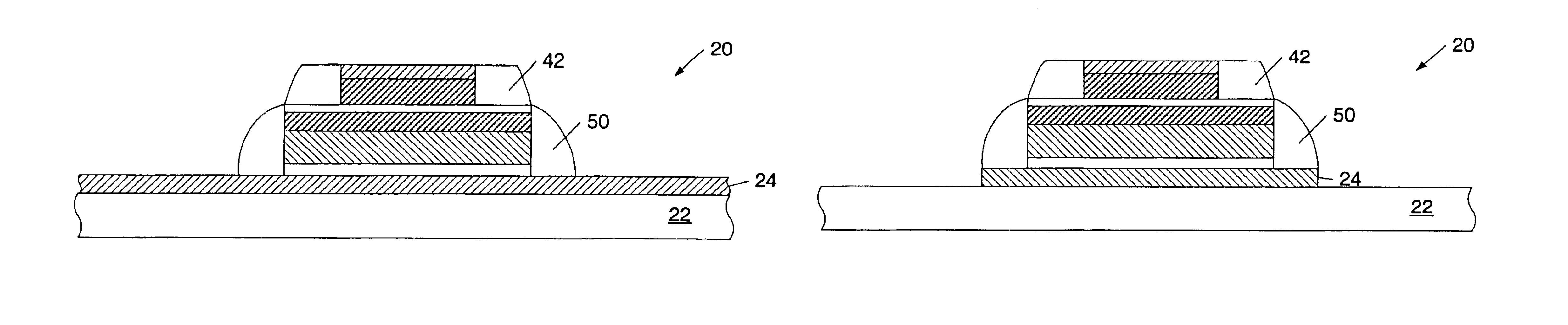
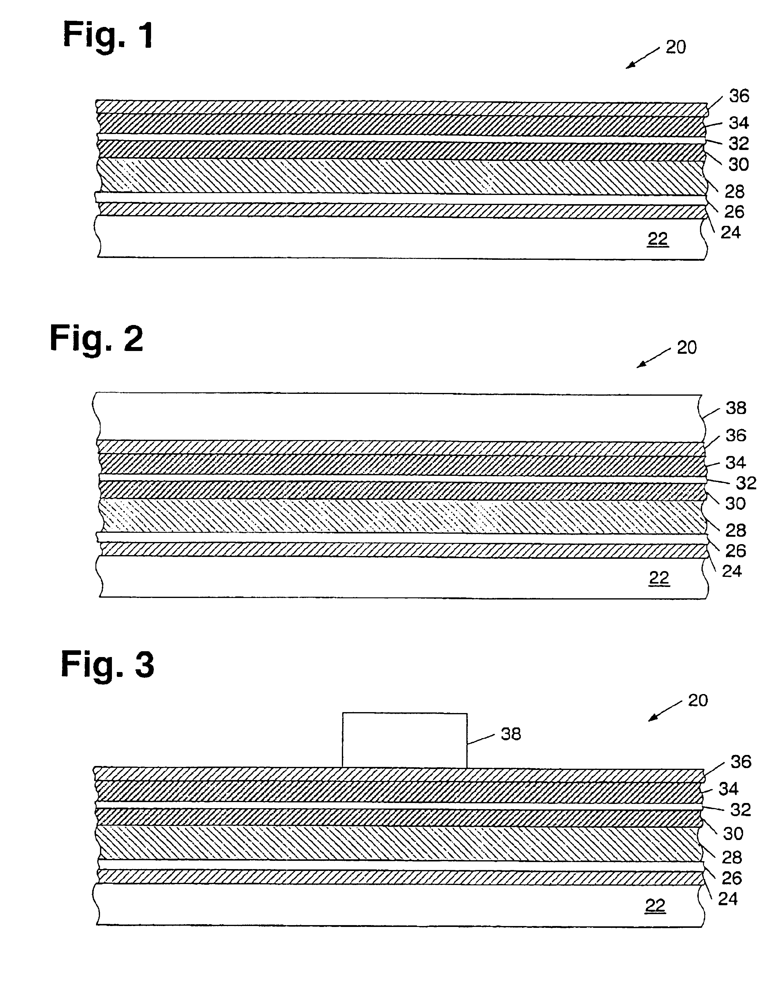
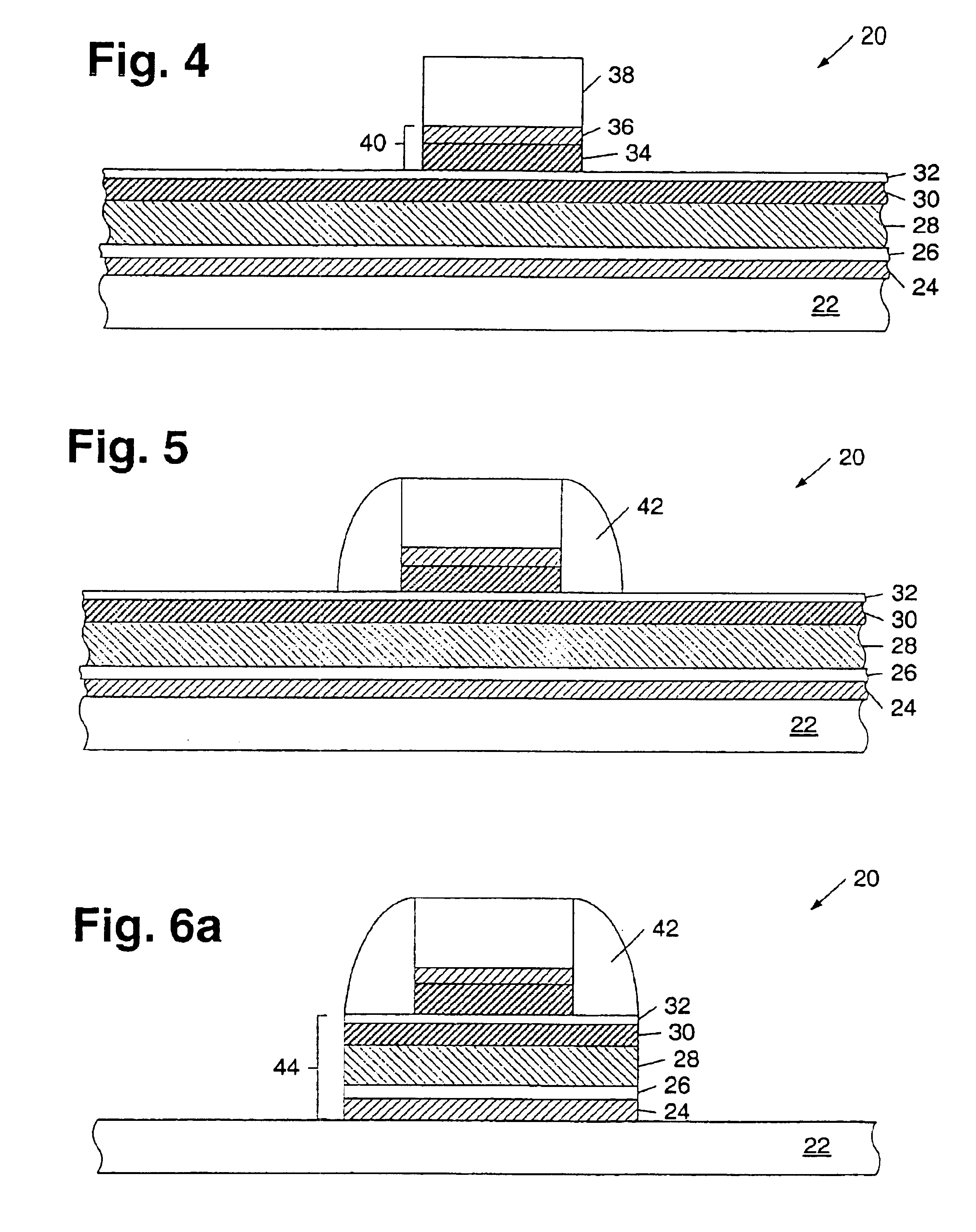
[0040]Turning to the drawings, exemplary embodiments of methods for processing a semiconductor topography are shown in FIGS. 1-15. In particular, methods for patterning one or more metal layers arranged above a metal insulating layer are provided. In addition, methods of producing a magnetic tunneling junction (MTJ) stack within a semiconductor device are provided. FIG. 1 depicts a partial cross-sectional view of semiconductor topography 20 in layers 22-36 formed upon and in contact with each other. In some embodiments, semiconductor topography 20 may include additional layers formed upon and in contact with one or more of layers 22-36. Alternatively, semiconductor topography 20 may include fewer layers than shown in FIG. 1. As such, it is noted that several layer configurations may be used for the method described herein. Semiconductor topographies 20 and 54 shown in FIGS. 1-11 are merely shown as exemplary embodiments. In particular, the composition, thickness, number, and arrange...


PUM

PropertyMeasurementUnit
widthaaaaaaaaaa
widthaaaaaaaaaa
thicknessaaaaaaaaaa

Abstract

A method for forming a magnetic tunneling junction (MJT) is provided. In some embodiments, the method may include patterning one or more magnetic layers to form an upper portion of a MTJ. The method may further include patterning one or more additional layers to form a lower portion of the MTJ. In some cases, the lower portion may include a tunneling layer of the MTJ having a width greater than the upper portion. In addition, in some embodiments the method may further include patterning an electrode below the lower portion. In some cases, the electrode may include a lowermost layer with a thickness equal to or less than approximately 100 angstroms. In addition or alternatively, the electrode may have a width greater than the width of the tunneling layer. In yet other embodiments, the method may include forming spacers along the sidewalls of the upper and / or lower portions.

Description

BACKGROUND OF THE INVENTION[0001]1. Field of the Invention[0002]This invention relates to semiconductor device manufacturing, and more particularly, to an alternative magnetic tunneling junction configuration and a method for making such a structure.[0003]2. Description of the Related Art[0004]The following descriptions and examples are not admitted to be prior art by virtue of their inclusion within this section.[0005]At various stages in the fabrication of semiconductor devices, it may be necessary to pattern one or more layers to form a semiconductor feature. Such a semiconductor feature may include, for example, a gate structure, an interconnect line, or a magnetic tunneling junction (MTJ) stack. The process parameters used for such a patterning process may affect the operation of the device comprising the semiconductor feature. For example, plasma etch techniques, which are typically used for metal etch processes, generally require temperatures greater than approximately 200° C...

Claims


Application Information

Patent Timeline
Patent Type & Authority Patents(United States)
IPC IPC(8): H01L29/66H01L29/788H01F10/32H01L43/12
CPCB82Y25/00H01L43/12H01F10/3254H10N50/01
Inventor SCHWARZ, BENJAMIN C. E.OUNADJELA, KAMEL
Owner CENT NAT DE LA RECHERCHE SCI
Why Eureka
Try Eureka