Substrate processing equipment and alignment control method of to-be-processed substrate

A technology of processing equipment and control method, which is applied in semiconductor/solid-state device manufacturing, instruments, electrical components, etc., and can solve the problems of poor reflective performance of alignment marks and inaccurate alignment results, etc.

Inactive Publication Date: 2017-05-24
BOE TECH GRP CO LTD +1
View PDF14 Cites 15 Cited by
  • Summary
  • Abstract
  • Description
  • Claims
  • Application Information

AI Technical Summary

Problems solved by technology

[0006] Embodiments of the present invention provide a substrate processing equipment and a method for controlling the alignment of substrates to be processed, which can solve the problem of inaccurate alignment results due to poor reflective performance of alignment marks when substrate processing equipment aligns substrates to be processed question

Method used


Image

  • Substrate processing equipment and alignment control method of to-be-processed substrate
  • Substrate processing equipment and alignment control method of to-be-processed substrate
  • Substrate processing equipment and alignment control method of to-be-processed substrate

Examples


Embodiment Construction

[0031] The following will clearly and completely describe the technical solutions in the embodiments of the present invention with reference to the accompanying drawings in the embodiments of the present invention. Obviously, the described embodiments are only some, not all, embodiments of the present invention. Based on the embodiments of the present invention, all other embodiments obtained by persons of ordinary skill in the art without making creative efforts belong to the protection scope of the present invention.

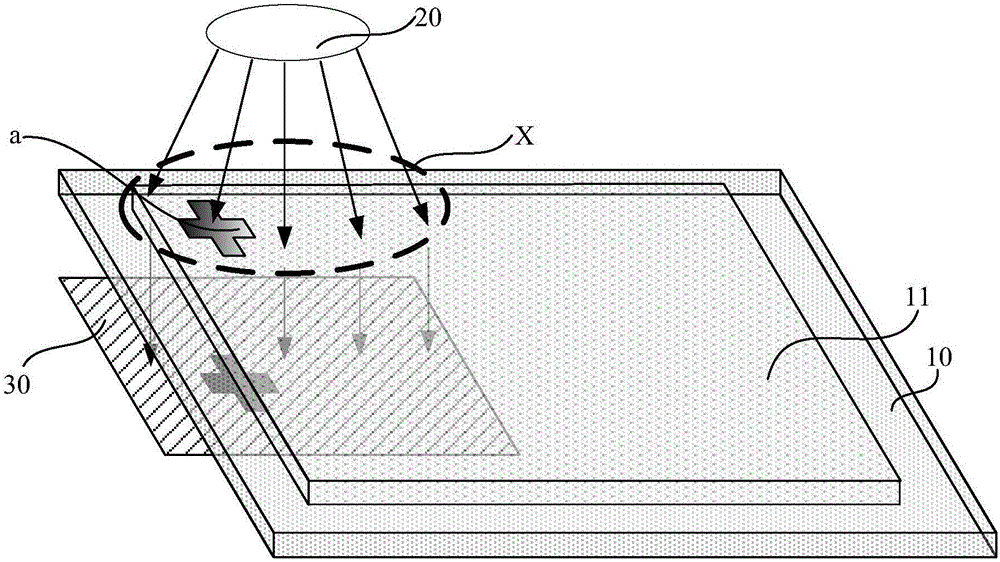
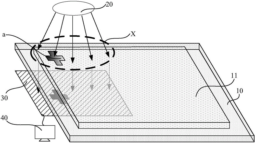
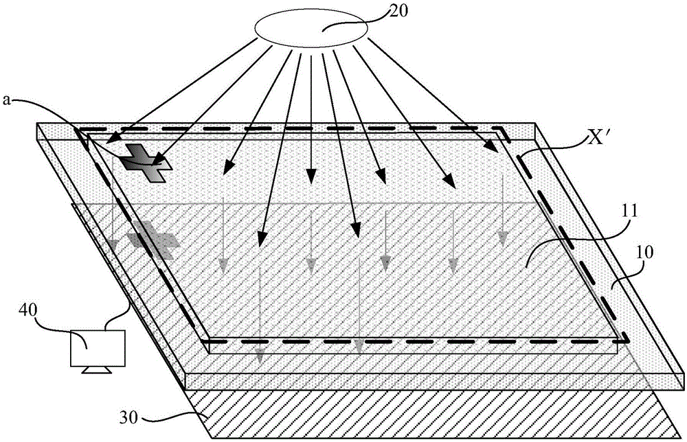
[0032] An embodiment of the present invention provides a substrate processing equipment, such as figure 1 As shown, it includes: a stage 10 for carrying a substrate 11 to be processed, an alignment mark a is provided on the substrate 11 to be processed, and the alignment mark a is a light-shielding material. The light source 20 is disposed on one side of the stage 10 . The image sensor 30 is disposed on the other side of the stage 10 . Wherein, the light sou...


PUM


Abstract

The embodiment of the invention provides substrate processing equipment and an alignment control method of a to-be-processed substrate, and relates to the semiconductor technical field. When the substrate processing equipment positions the to-be-processed substrate in the prior art, the alignment result may be inaccurate because alignment marks are poor in reflective performance; the substrate processing equipment can solve said problems, and comprises the following units: a carrier deck used for bearing the to-be-processed substrate, wherein the to-be-processed substrate has alignment marks made of shading material; a light source arranged on one side of the carrier deck; an image sensor arranged on the other side of the carrier deck, wherein the light source is used for sending lights to the to-be-processed substrate; the light reaches the image sensor through the to-be-processed substrate, the image sensor can collect the image containing the alignment marks; the irradiation zone of the light source at least covers the outer edges of the alignment marks.

Description

technical field [0001] The invention relates to the technical field of semiconductors, in particular to substrate processing equipment and a method for controlling alignment of substrates to be processed. Background technique [0002] TFT-LCD (Thin Film Transistor-Liquid Crystal Display, Thin Film Transistor-Liquid Crystal Display, Thin Film Transistor-Liquid Crystal Display) usually includes an array substrate and a color filter substrate that are boxed to each other, and a liquid crystal layer that is sealed between the array substrate and the color filter substrate that are boxed to each other. There are pixel electrodes and common electrodes for forming an electric field on the liquid crystal display panel, and an electric field is generated between the pixel electrodes and the common electrodes by applying a voltage to control the deflection direction of the liquid crystal molecules of the liquid crystal layer and control the polarization of incident light, thereby gener...

Claims


Application Information

Patent Timeline
IPC IPC(8): H01L21/68G02F1/13
CPCH01L21/681G02F1/1303
Inventor 李世维樊超王新华易熊
Owner BOE TECH GRP CO LTD
Why Eureka
Try Eureka