Pixel circuit, driving method of pixel circuit, display panel and display device

A technology for pixel circuits and drive transistors, applied in the fields of pixel circuits, display panels and display devices, capable of solving problems affecting image display effects, uneven display brightness, uneven brightness, etc.

Inactive Publication Date: 2017-05-31
BOE TECH GRP CO LTD
View PDF8 Cites 13 Cited by
  • Summary
  • Abstract
  • Description
  • Claims
  • Application Information

AI Technical Summary

Problems solved by technology

Due to reasons such as process technology and device aging, the threshold voltage V of the driving transistor of the pixel circuit will be th There is inhomogeneity, which causes the current flowing through each OLED to change, making the display brightness uneven, which affects the display effe

Method used


Image

  • Pixel circuit, driving method of pixel circuit, display panel and display device
  • Pixel circuit, driving method of pixel circuit, display panel and display device
  • Pixel circuit, driving method of pixel circuit, display panel and display device

Examples


Embodiment 1

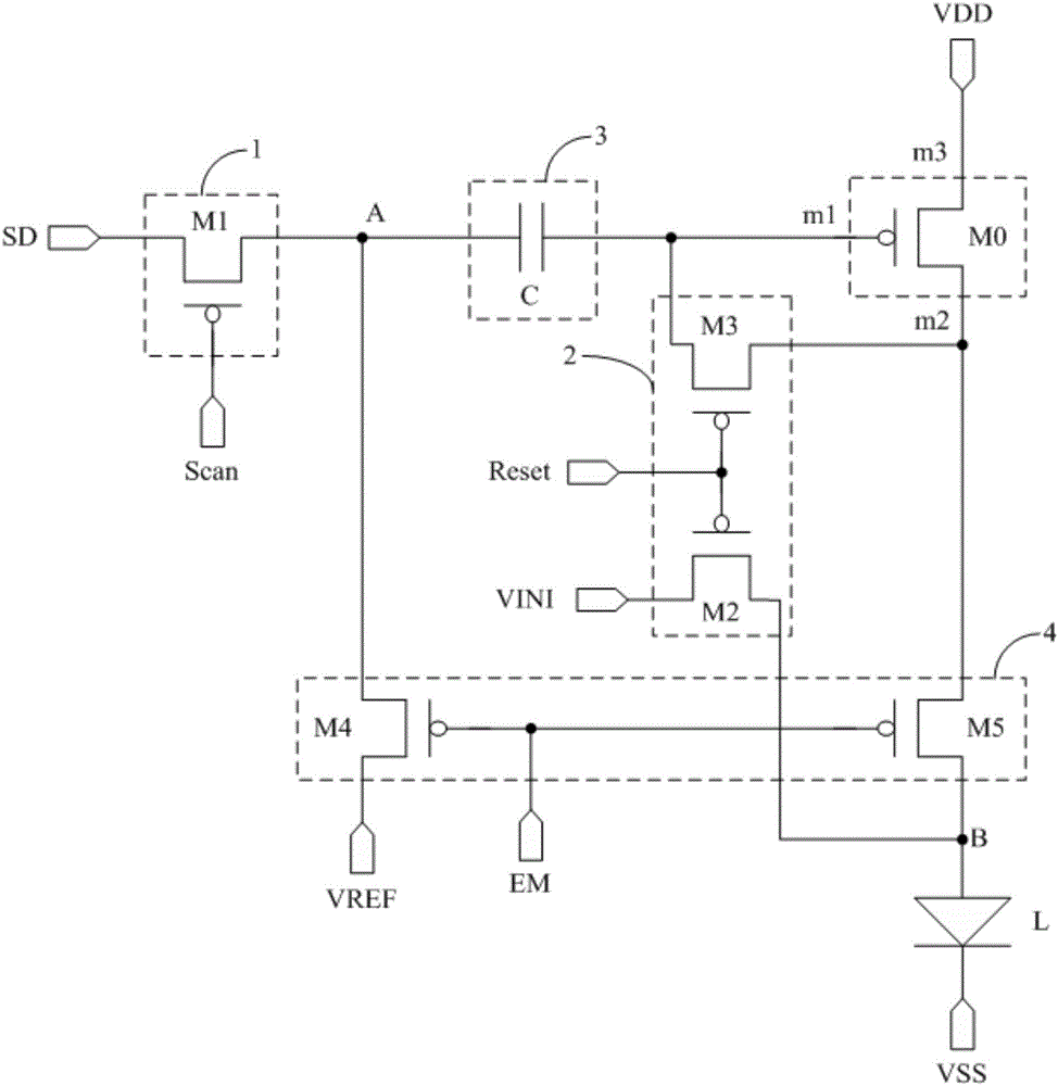
[0078] Such as Figure 2a As shown, the drive transistor M0 is a P-type transistor, and all switching transistors are P-type transistors; the corresponding input timing diagram is shown in Figure 4a shown. Specifically, choose the Figure 4a The three stages T1, T2 and T3 in the input timing diagram shown.

[0079] In the T1 stage, Scan=1, Reset=0, EM1=0.

[0080] Since Scan=1, the first switching transistor M1 is turned off. Since Reset=0, both the second switch transistor M2 and the third switch transistor M3 are turned on. Since EM1=0, both the fourth switch transistor M4 and the fifth switch transistor M5 are turned on. The turned-on fourth switch transistor M4 provides the signal of the reference signal terminal VREF to the first node A, so the voltage of the first node A is the voltage V of the signal of the reference signal terminal VREF ref . The turned-on fifth switching transistor M5 may turn on the drain of the driving transistor M0 and the second node B. Re...

Embodiment 2

[0086] Such as Figure 3a As shown, the driving transistor M0 is an N-type transistor, and all switching transistors are N-type transistors; the corresponding input timing diagram is shown in Figure 4b shown. Specifically, choose the Figure 4b The three stages T1, T2 and T3 in the input timing diagram shown.

[0087] In the T1 stage, Scan=0, Reset=1, EM1=1.

[0088] Since Scan=0, the first switching transistor M1 is turned off. Since Reset=1, both the second switch transistor M2 and the third switch transistor M3 are turned on. Since EM1=1, both the fourth switch transistor M4 and the fifth switch transistor M5 are turned on. The turned-on fourth switch transistor M4 provides the signal of the reference signal terminal VREF to the first node A, so the voltage of the first node A is the voltage V of the signal of the reference signal terminal VREF ref . The turned-on fifth switching transistor M5 may turn on the source of the driving transistor M0 and the second node B...


PUM


Abstract

The invention provides a pixel circuit, a driving method of the pixel circuit, a display panel and a display device. The pixel circuit comprises a data writing module, a compensation control module, a storage module, a luminescence control module, a driver transistor and a luminous device. In the cooperation of the four modules and the driver transistor, a working current used for making the driver transistor drive the luminous device to give out light in the pixel circuit is only correlated with the voltage at the data signal end and the voltage at a reference signal end, and uncorrelated with the threshold voltage of the driver transistor and the voltage of a first power source end so that the working current flowing through the luminous device can be avoided from being affected by the threshold voltage of the driver transistor and IR Drop, accordingly the working current driving the luminous device to give out light keeps stable, and then the uniformity of screen brightness in a display area in the display device can be improved.

Description

technical field [0001] The present invention relates to the field of display technology, in particular to a pixel circuit, a driving method thereof, a display panel and a display device. Background technique [0002] Organic Light Emitting Diode (OLED) is one of the hot spots in the field of flat panel display research today. Compared with Liquid Crystal Display (LCD), OLED display has low energy consumption, low production cost, self-illumination, and wide viewing angle. and quick response. At present, OLED displays have begun to replace traditional LCD displays in display fields such as mobile phones, tablet computers, and digital cameras. [0003] Unlike LCDs that use a stable voltage to control brightness, OLEDs are driven by current and require a stable current to control their light emission. Due to reasons such as process technology and device aging, the threshold voltage V of the driving transistor of the pixel circuit will be th There is inhomogeneity, which caus...

Claims


Application Information

Patent Timeline
IPC IPC(8): G09G3/3233G09G3/3241
CPCG09G3/3233G09G3/3241G09G2320/0233
Inventor 马占洁
Owner BOE TECH GRP CO LTD
Why Eureka
Try Eureka