mr sensor and card reader
A sensor and card reader technology, applied in the field of MR sensors, can solve problems such as inability to obtain signals, and achieve the effects of cost reduction and simple structure
- Summary
- Abstract
- Description
- Claims
- Application Information
AI Technical Summary
Problems solved by technology
Method used
Image

Examples
Embodiment approach 1
[0042] (Schematic structure of the card reader)
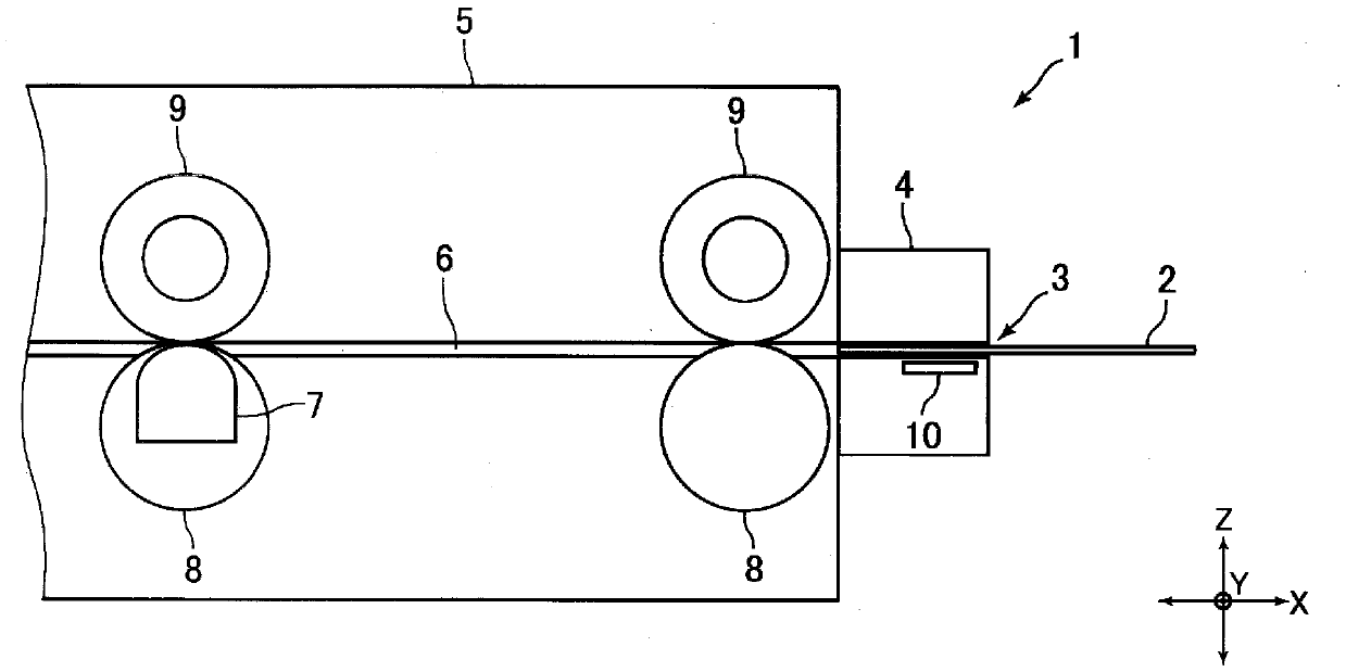
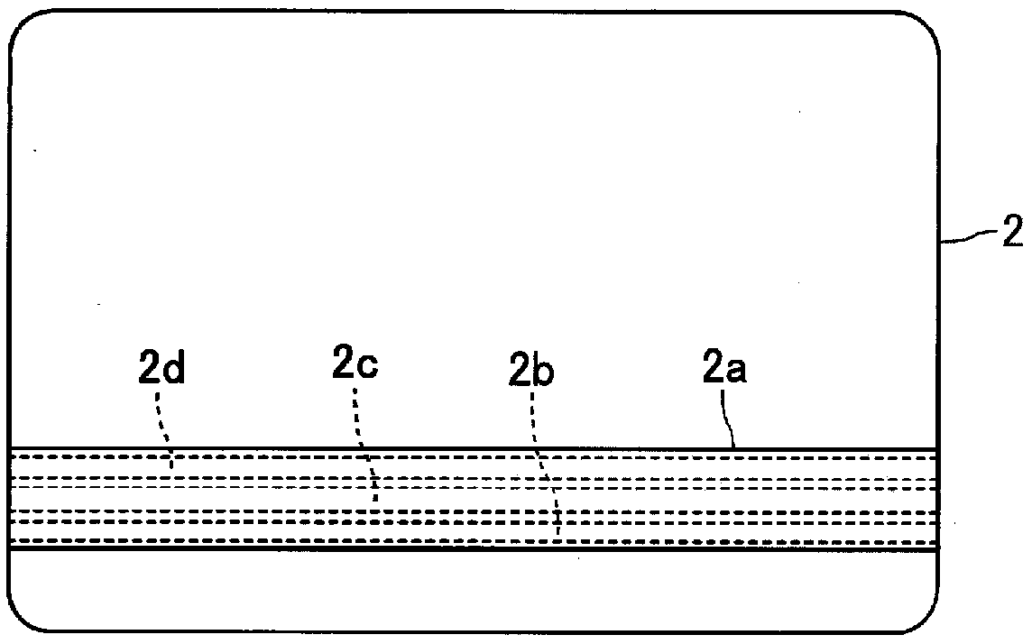
[0043] figure 1 It is a schematic diagram of the card reader 1 concerning embodiment of this invention. figure 2 is showing figure 1 A view of the back of the card 2 is shown.
[0044] The card reader 1 of the present embodiment is a device for reading magnetic data recorded on the card 2 or recording magnetic data on the card 2, and is used by being installed in a predetermined high-level device such as an ATM, for example. This card reader 1 has: a card insertion portion 4 formed with a card insertion opening 3 into which a card 2 is inserted; and a main body portion 5 . Inside the card reader 1, a card passage 6 through which the card 2 inserted through the card insertion port 3 passes is formed.
[0045] In this embodiment, the card 2 is figure 1 The X direction shown is passed through. That is, the X direction is the passing direction of the card 2 . And, orthogonal to the X direction figure 1 The Z direction is t...
Embodiment approach 2
[0074] (Structure of MR sensor)
[0075] Figure 7 It is a plan view of the MR sensor 10 according to Embodiment 2 of the present invention. Figure 8 yes Figure 7 A graph of an example of the output signal of the MR sensor 10 is shown.
[0076] In Embodiment 1 and Embodiment 2, the structure of the MR sensor 10 is different. Therefore, below, the configuration of the MR sensor 10 according to the second embodiment will be described focusing on differences between the configuration of the MR sensor 10 according to the second embodiment and the configuration of the MR sensor 10 according to the first embodiment. In addition, in Figure 7 In, the same code|symbol is attached|subjected to the same structure as Embodiment 1.
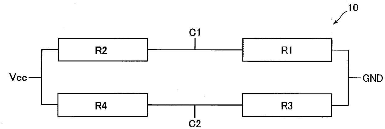
[0077] Like the MR sensor 10 of Embodiment 1, the MR sensor 10 of this embodiment has a resistor R1 and a resistor R2 connected in series to each other, and a resistor R3 and a resistor R4 connected in series to each other. The resistor R1 and the res...
Embodiment approach 3
[0092] (Structure of MR sensor)
[0093] Figure 9 It is a plan view of the MR sensor 10 according to Embodiment 3 of the present invention. Figure 10 (A) is shown Figure 9 The graph showing the relationship between the resistance change rates α1 and α2 of the resistors R1 to R4 and the magnetic flux density, Figure 10 (B) is shown in the Figure 10 (A) The resistance change rate α1 of resistors R2 and R3 when the magnetic flux density is a specified value; the resistance change rate α2 of resistors R1 and R4; and the resistance change rate α1 of resistors R2 and R3 , A list of the ratio of the resistance change rate α2 of R4. Figure 11 is showing Figure 9 A graph of an example of the output signal of the MR sensor 10 is shown.
[0094] In Embodiments 1, 2, and 3, the structure of the MR sensor 10 is different. Therefore, the configuration of the MR sensor 10 according to Embodiment 3 will be described below focusing on differences between the configuration of MR s...
PUM
| Property | Measurement | Unit |
|---|---|---|
| thickness | aaaaa | aaaaa |
| thickness | aaaaa | aaaaa |
Abstract
Description
Claims
Application Information
 - R&D
- Intellectual Property
- Life Sciences
- Materials
- Tech Scout
- Unparalleled Data Quality
- Higher Quality Content
- 60% Fewer Hallucinations
Browse by: Latest US Patents, China's latest patents, Technical Efficacy Thesaurus, Application Domain, Technology Topic, Popular Technical Reports.
© 2025 PatSnap. All rights reserved.Legal|Privacy policy|Modern Slavery Act Transparency Statement|Sitemap|About US| Contact US: help@patsnap.com