Micro luminous display device and manufacturing method thereof

A manufacturing method and luminescent display technology, applied to identification devices, static indicators, instruments, etc., can solve the problems of time-consuming, low mass production, etc.

Active Publication Date: 2017-06-09
INNOLUX CORP
View PDF3 Cites 17 Cited by
  • Summary
  • Abstract
  • Description
  • Claims
  • Application Information

AI Technical Summary

Problems solved by technology

Among them, the method of setting micro-LED chips is generally to adopt single pick-and-place (pick-and-place). However, the display device easily has hundre

Method used


Image

  • Micro luminous display device and manufacturing method thereof
  • Micro luminous display device and manufacturing method thereof
  • Micro luminous display device and manufacturing method thereof

Examples


no. 1 example

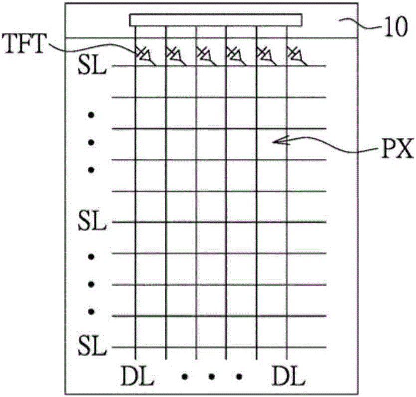
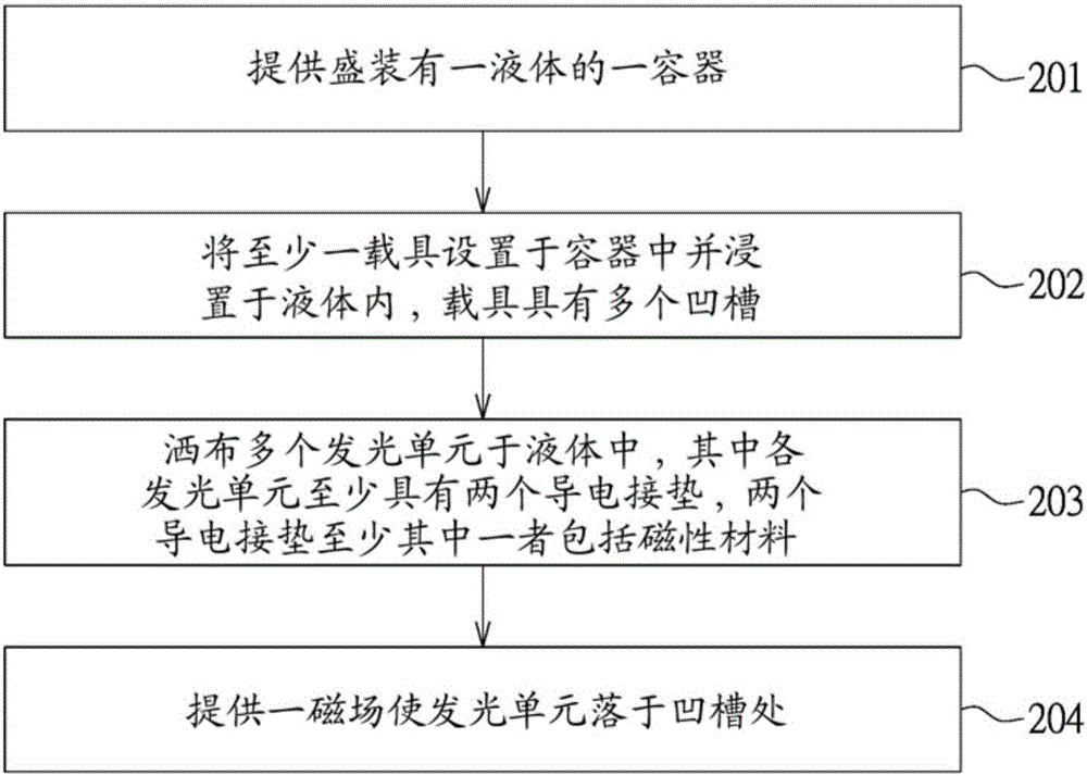
[0061] Figure 3A-Figure 3D It is a schematic diagram of an arrangement method of light emitting units of a micro light emitting display device according to the first embodiment of the present disclosure. First, provide a container 30 containing a liquid 31 and a carrier 40 with a plurality of grooves 42, such as Figure 3A shown. And provide a plurality of light emitting units 20 such as micro light emitting diode chips. Wherein, the arrangement of the grooves 42 of the carrier 40 may correspond to the sub-pixel arrangement of the display device; for example, if the driving element (ex: thin film transistor) of the applied display device is Figure 1A As shown in the array, the grooves 42 can also be distributed in an array and their positions correspond to the thin film transistors in the sub-pixel area. The groove 42 is made, for example, by forming several sunken regions on the upper surface 401 of the carrier 40 . According to some embodiments, at a position correspond...

no. 2 example

[0075] except as Figure 3A-Figure 3D The shown carrier 40 is placed flat on the bottom of the container 30 and is parallel to the horizontal plane (i.e.XY plane). The carrier 40 placed in the bottom of the container 30 can also form an angle θ with the horizontal plane (i.e.XY plane), for example, 0 Figure 3A-3D The carrier 40 is shown at an angle θ=0 to the horizontal plane. Although in the second embodiment, the bottom of the container 30 is used as an inclined surface to form an angle θ of less than 90 degrees with the XY plane, the present invention is not limited thereto.

[0076] The same or similar reference numerals are used for the same or similar elements of the second embodiment and the first embodiment. For details of the same components and steps in the second embodiment, please refer to the content of the first embodiment, and will not be repeated here.

[0077] Figure 5 It is a schematic diagram of arrangement of light emitting units of a micro light emitt...

no. 3 example

[0083] Figure 6A-6D It is a schematic diagram of an arrangement method of light emitting units of a micro light emitting display device according to the third embodiment of the present disclosure. The difference between the third embodiment and the first embodiment is mainly that the carrier 40 is disposed in the container 30 . like Figure 6A As shown, the carrier 40 is disposed on the side wall 302 of the container 30 and is perpendicular to the bottom 301 of the container 30 , and the carrier 40 has a plurality of grooves 42 . The arrangement and size design of the grooves 42 are as mentioned above, and will not be repeated here.

[0084] Sprinkle the light-emitting unit 20 in the liquid 31, and provide an external magnetic field to force the magnetic material to control the light-emitting unit 20 to fall into the groove 42, as Figure 6B-1 / 6B-2. In the third embodiment, the applied magnetic field at least includes a magnetic field direction (X direction) perpendicula...


PUM


Abstract

The invention discloses a micro luminous display device and a manufacturing method thereof. The manufacturing method comprises the following steps: providing a tank containing a liquid; disposing at least a carrying plate with several recessed regions in the tank, and the carrying plate being immersed in the liquid; dropping several lighting devices into the liquid, wherein each of the lighting devices includes at least two conductive pads, and one of the two conductive pads includes a magnetic material; applying a magnetic field for the lighting devices and the lighting devices will dispose within the recessed regions of the carrying plate; removing the carrying plate with the lighting devices out of the tank, and electrically assembling the lighting devices to an array substrate.

Description

technical field [0001] The invention relates to a micro light emitting display device and a manufacturing method thereof, and in particular to a micro light emitting unit and an arrangement method thereof. Background technique [0002] Electronic products with display devices have become an indispensable necessity for modern people, whether in work, study, or personal leisure and entertainment, including smart phones (SmartPhone), tablet computers (Pad), notebook computers (Notebook) , Monitor (Monitor) to TV (TV) and many other related products. With the vigorous development of portable display device products, display device products have more and more requirements for functions, specifications and costs. Energy-saving and environmentally friendly display device technologies are the focus of the development of next-generation new display devices. [0003] Display device In terms of panel display technology, in addition to the mature liquid crystal display technology, its ...

Claims


Application Information

Patent Timeline
IPC IPC(8): H01L27/32G09F9/33G09G3/3208
CPCG09F9/33G09G3/3208G09G3/3225G09G3/3648H10K59/00H10K59/12
Inventor 陈柏锋谢朝桦刘同凯
Owner INNOLUX CORP
Why Eureka
Try Eureka