Manufacturing method of OLED panel and OLED panel

A manufacturing method and panel technology, applied in the field of OLED display, can solve the problems of ink overflow, difficulty in OLED panels, printing OLED light-emitting devices, etc., and achieve the effects of improving resolution and reducing lateral leakage.

Inactive Publication Date: 2017-06-13
SHENZHEN CHINA STAR OPTOELECTRONICS SEMICON DISPLAY TECH CO LTD
View PDF6 Cites 0 Cited by
  • Summary
  • Abstract
  • Description
  • Claims
  • Application Information

AI Technical Summary

Problems solved by technology

However, due to the limitation of current printing capabilities, it is very difficult to use printing technology to produce high-resolution (such as 4K) OLED panels, mainly because the existing printing methods cannot perfectly print OLED light in a very small pixel unit The device 202 will cause ink overflow, causing color mixing and other defects

Method used


Image

  • Manufacturing method of OLED panel and OLED panel
  • Manufacturing method of OLED panel and OLED panel
  • Manufacturing method of OLED panel and OLED panel

Examples


Embodiment Construction

[0032] In order to further illustrate the technical means adopted by the present invention and its effects, the following describes in detail in conjunction with preferred embodiments of the present invention and accompanying drawings.

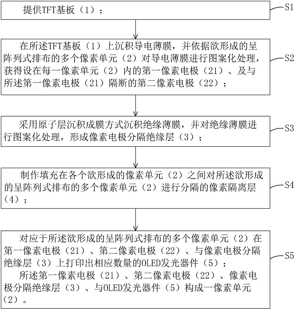
[0033] see image 3 , combined with Figure 4 ,and Figure 5 , the present invention at first provides a kind of manufacturing method of OLED panel, comprises the following steps:

[0034] Step S1 , providing a TFT substrate 1 .

[0035] Specifically, the thickness of the TFT substrate 1 is It usually includes a glass substrate, a gate, a scanning line, a gate insulating layer, an active layer, an interlayer insulating layer, a source, a drain, a data line, etc., which are the same as those in the prior art and will not be described here.

[0036] Step S2, depositing a conductive film on the TFT substrate 1, and patterning the conductive film according to the plurality of pixel units 2 arranged in an array to obtain the first pixel unit 2...


PUM


Abstract

The invention provides a manufacturing method of an OLED panel and the OLED panel. The manufacturing method of the OLED panel comprises the steps of manufacturing a first pixel electrode (21) and a second pixel electrode (22) in each pixel unit (2), and depositing an insulating thin film by adopting an atomic layer deposition film-forming mode, and then carrying out patterning treatment to form a pixel electrode partition insulation layer (3); filling a longitudinal part (31) of the pixel electrode partition insulation layer (3) between the first pixel electrode (21) and the second pixel electrode (22), covering the part, relatively close to the second pixel electrode (22), of the first pixel electrode (21) and the part, relatively close to the first pixel electrode (21), of the second pixel electrode (22) with two ends of a transverse part (22) separately and then manufacturing a pixel isolation layer (4); and finally printing an OLED light-emitting device (5). The resolution of the OELD panel can be improved without changing the printing accuracy so that the first pixel electrode (21) and the second pixel electrode (22) are fully insulated.

Description

technical field [0001] The invention relates to the field of OLED display technology, in particular to a method for manufacturing an OLED panel and the OLED panel. Background technique [0002] Organic Light Emitting Diode (OLED) panel has self-illumination, low driving voltage, high luminous efficiency, short response time, high definition and contrast, nearly 180° viewing angle, wide operating temperature range, and can realize flexible display and large It is recognized by the industry as a display device with the most potential for development due to its many advantages such as full-color display. [0003] Please also see figure 1 and figure 2 , the existing OLED panel generally includes a TFT substrate 100, a plurality of pixel units 200 arranged in an array on the TFT substrate 100, and filling between each pixel unit 200 for the pixel units 200 arranged in an array. A plurality of pixel units 200 are separated by a pixel isolation layer 300 , wherein each pixel un...

Claims


Application Information

Patent Timeline
IPC IPC(8): H01L27/32H01L51/50H01L51/56
CPCH10K59/121H10K59/122H10K71/00
Inventor 张晓星
Owner SHENZHEN CHINA STAR OPTOELECTRONICS SEMICON DISPLAY TECH CO LTD
Why Eureka
Try Eureka