Test motherboard usable for various chip packaging forms and test method
A technology of chip packaging and form, applied in the direction of electronic circuit testing, measuring electricity, measuring devices, etc., to achieve the effect of shortening the development time
- Summary
- Abstract
- Description
- Claims
- Application Information
AI Technical Summary
Problems solved by technology
Method used
Image

Examples
Embodiment Construction
[0023] Below in conjunction with accompanying drawing and embodiment the present invention will be further described:
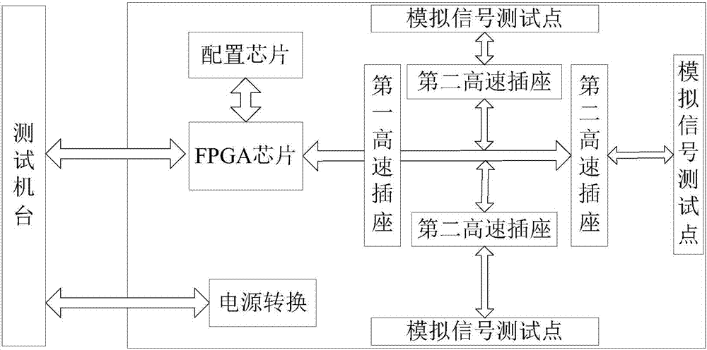
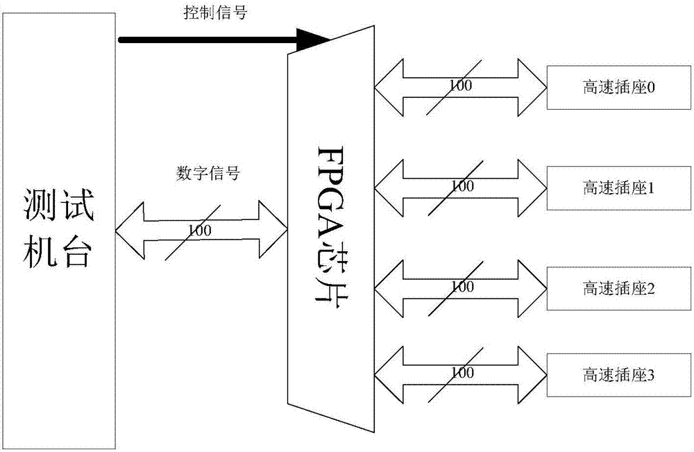
[0024] This test motherboard is mainly used as a conversion bridge between the test machine and the test sub-board. The test motherboard connects the FPGA to the test machine through a fixed interface. The high-speed socket and the second high-speed socket) are connected to the test sub-board, and by configuring FPGA internal logic conversion, the test machine can test different functions of different chips.
[0025] Such as figure 1 As shown, a kind of test mother board that can be used for multiple chip package forms, comprises programmable chip (the present embodiment takes FPGA chip as example), and described FPGA chip is reserved the interface that is connected with test machine; Said FPGA The chip is connected with the configuration chip and the first high-speed socket, and the first high-speed socket is connected with three second high-speed sockets; ...
PUM
 Abstract
Description
Claims
Application Information
 - Generate Ideas
- Intellectual Property
- Life Sciences
- Materials
- Tech Scout
- Unparalleled Data Quality
- Higher Quality Content
- 60% Fewer Hallucinations
Browse by: Latest US Patents, China's latest patents, Technical Efficacy Thesaurus, Application Domain, Technology Topic, Popular Technical Reports.
© 2025 PatSnap. All rights reserved.Legal|Privacy policy|Modern Slavery Act Transparency Statement|Sitemap|About US| Contact US: help@patsnap.com