Display panel mother board and manufacturing method of display panel
A display panel and motherboard technology, applied in glass manufacturing equipment, manufacturing tools, identification devices, etc., can solve problems such as uneven support force, deterioration of cutting cracks, etc., achieve uniform pressure, reduce deterioration of cutting cracks, and stabilize support Effect
- Summary
- Abstract
- Description
- Claims
- Application Information
AI Technical Summary
Problems solved by technology
Method used
Image
Examples
Embodiment 1
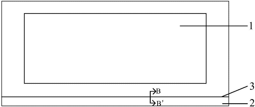
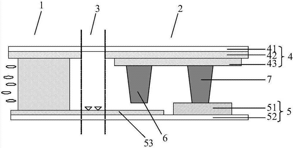
[0037] Please refer to image 3 , this embodiment provides a display panel motherboard, including a first substrate 4 and a second substrate 5 arranged in a box, the first substrate 4 and the second substrate 5 include a display area 1 and a non-display area 2 located outside the display area 1, In the non-display area 2 of the first substrate 4, a first spacer 6 and a second spacer 7 are sequentially arranged on the first substrate 4 along a direction away from the display area 2; wherein the first spacer 6 is close to The vertical distance from the end face of the second substrate 5 to the surface of the second substrate 5 close to the first substrate 4 is d1; The vertical distance is d2, wherein, d1=d2, so that when the display panel mother board is cut to form a display panel, the pressure on the position corresponding to the first spacer 6 on the first substrate 4 and the pressure on the position corresponding to the second spacer The pressure on the corresponding positi...
Embodiment 2
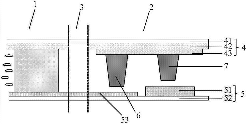
[0047] Please refer to Figure 4 , this embodiment provides a display panel motherboard, which has a structure similar to that of the display panel motherboard in Embodiment 1, the difference between it and Embodiment 1 is that d1 and d2 are equal to zero.
[0048] Compared with the prior art, in this embodiment, the height of the second spacer 7 is kept constant, and at the same time, the height of the first spacer 6 is increased, so that the height of the first spacer 6 is greater than that of the first spacer 6. The height of the two spacers 7, so that d1 and d2 are equal to zero. Certainly, the first spacer 6 and the second spacer 7 can be manufactured through a single process using a half-level mask, without adding an additional manufacturing process, which will not be repeated here.
[0049] In other words, in this embodiment, both the first spacer 6 and the second spacer 7 are in contact with the second substrate 5, that is, the first spacer 6 and the second spacer 7 a...
Embodiment 3
[0052] Please refer to Figure 5 , this embodiment provides a display panel motherboard, which has a structure similar to that of the display panel motherboard of Embodiment 1 or 2, and its difference from Embodiment 1 or 2 is that the first substrate 4 is close to the second substrate 5 One side includes a black matrix pattern 42 and a colored resin pattern 43 arranged in sequence, the colored resin pattern 43 is provided with a first through groove 44 , and part of the second spacer 7 is located in the first through groove 44 .
[0053] It should be noted that the depth of the first through groove 44 in this embodiment is equal to the thickness of the colored resin pattern 43, specifically, the side of the first substrate 4 close to the second substrate 5 (ie Figure 5 The lower part of the first substrate 41) includes a colored resin pattern 43 provided with a first through groove 44, and the first through groove 44 accommodates the part of the second spacer 7 away from the...
PUM
 Abstract
Description
Claims
Application Information


