Spiral stacked integrated inductor and transformer

A spiral, stacked technology, applied in inductors, fixed inductors, semiconductor devices, etc., can solve the problem of occupying a large chip area, achieve high symmetry, save component area, and reduce winding complexity.

Active Publication Date: 2019-05-10
REALTEK SEMICON CORP
View PDF7 Cites 0 Cited by
  • Summary
  • Abstract
  • Description
  • Claims
  • Application Information

AI Technical Summary

Problems solved by technology

However, inductors and transformers in integrated circuits often occupy a large amount of chip area. Therefore, how to reduce the area of ​​inductors and transformers in integrated circuits while maintaining the characteristics of components, such as inductance, quality factor (Q) and coupling coefficient (coupling coefficient, K), etc., have become an important topic

Method used


Image

  • Spiral stacked integrated inductor and transformer
  • Spiral stacked integrated inductor and transformer
  • Spiral stacked integrated inductor and transformer

Examples


Embodiment Construction

[0017] The technical terms in the following explanations refer to the customary terms in this technical field. If some terms are explained or defined in this manual, the explanations or definitions of this part of the terms shall prevail.

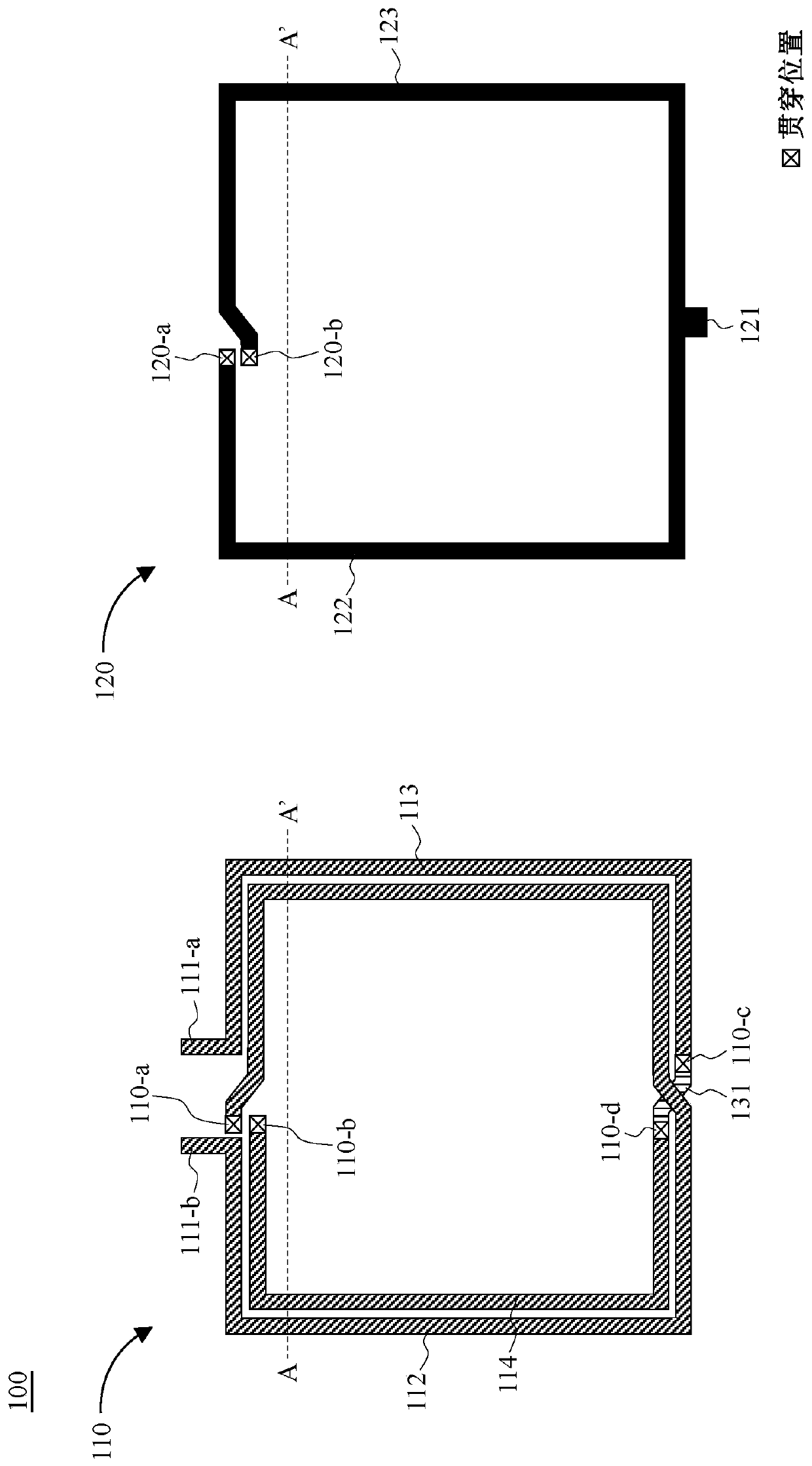
[0018] figure 1 It is a structural diagram of an embodiment of the spiral stacked integrated inductor of the present invention. The helical stacked integrated inductor 100 is composed of a helical coil 110 and a helical coil 120. Most of the metal wire segments of the helical coil 110 are located in the first metal layer in the semiconductor structure, and most of the metal wire segments of the helical coil 120 are located in the The second metal layer in the semiconductor structure, that is, the helical coil 110 is substantially located on the plane of the first metal layer, and the helical coil 120 is substantially located on the plane of the second metal layer. The helical coil 110 has an end point 111 - a and an end point 111 - b and i...


PUM


Abstract

The invention relates to a spiral stacked bulk inductor and transformer. The spiral stacked bulk inductor is composed of a first induction unit and a second induction unit and comprises a first spiral coil and a second spiral coil; the first spiral coil is actually located on a first plane and provided with a first outer coil body and a first inner coil body, the first inner coil body is located in the first outer coil body, and one part of the first induction unit and one part of the second induction part is formed by the first spiral coil; the second spiral coil is actually located on a second plane different from the first plane, has an overlapping range with the first spiral coil, and one part of the first induction unit and one part of the second induction unit are formed by the second spiral coil. The first spiral coil and the second spiral coil are arranged in a staggered mode.

Description

technical field [0001] The invention relates to transformers and inductors, in particular to a spiral stacked integrated transformer and a spiral stacked integrated inductor. Background technique [0002] Inductors and transformers are important components used in radio frequency integrated circuits to achieve single-ended to differential signal conversion, signal coupling, impedance matching and other functions. With the development of integrated circuits to System on Chip (SoC), integrated inductors (integrated inductor) and integrated transformer (integrated transformer) have gradually replaced traditional discrete components, and are widely used in radio frequency integrated circuits. However, inductors and transformers in integrated circuits often occupy a large amount of chip area. Therefore, how to reduce the area of ​​inductors and transformers in integrated circuits while maintaining the characteristics of components, such as inductance, quality factor (Q) And coup...

Claims


Application Information

Patent Timeline
Patent Type & Authority Patents(China)
IPC IPC(8): H01F17/00H01F27/28H01L23/64
Inventor 颜孝璁
Owner REALTEK SEMICON CORP
Why Eureka
Try Eureka