Device packaging structure and preparation method therefor

A technology for device packaging and encapsulation, which is applied in the manufacturing of semiconductor/solid-state devices, electric solid-state devices, semiconductor devices, etc., and can solve the problem that the second encapsulant is easy to cross over.

Inactive Publication Date: 2017-06-30
BOE TECH GRP CO LTD
View PDF4 Cites 9 Cited by
  • Summary
  • Abstract
  • Description
  • Claims
  • Application Information

AI Technical Summary

Problems solved by technology

[0005] However, in the prior art, if the lamination pressure is too high during the lamination process of the pa

Method used


Image

  • Device packaging structure and preparation method therefor
  • Device packaging structure and preparation method therefor
  • Device packaging structure and preparation method therefor

Examples


Embodiment Construction

[0028] The following will clearly and completely describe the technical solutions in the embodiments of the present invention with reference to the accompanying drawings in the embodiments of the present invention. Obviously, the described embodiments are only some, not all, embodiments of the present invention. Based on the embodiments of the present invention, all other embodiments obtained by persons of ordinary skill in the art without making creative efforts belong to the protection scope of the present invention.

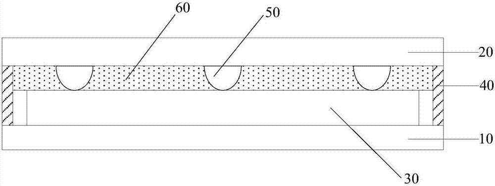
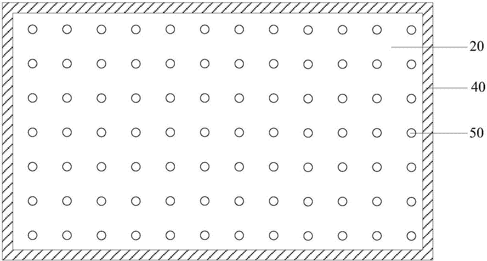
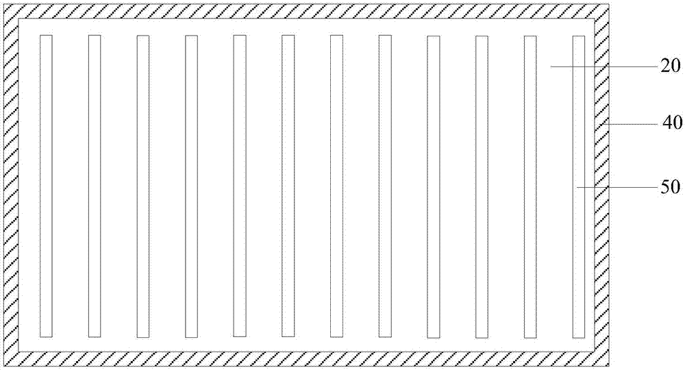
[0029] During fabrication of the device package structure, a first encapsulant is formed on the edge of the package cover, and then the area defined by the first encapsulant is filled with a second encapsulant, and then the package cover and the base substrate are bonded together. In order to make the package cover and the base substrate bondable, before the package cover and the base substrate are bonded, the first encapsulant and the second encapsulant are on...


PUM

PropertyMeasurementUnit
Diameteraaaaaaaaaa

Abstract

The embodiment of the invention provides a device packaging structure and a preparation method therefor, and relates to the technical field of display. The structure can prevent first packaging glue from washing first packaging glue away during the stitching of a substrate and a packaging cover plate because of the excessive stitching pressure. The structure comprises the substrate and the packaging cover plate, which are set oppositely; a to-be-packaged device formed on the substrate; the first packaging glue which is formed at the edge of the packaging cover plate, and is used for enabling the packaging cover plate and the substrate to be connected to form a closed space, wherein the to-be-packaged device is located in the closed space; a plurality of supporting parts which are formed on the packaging cover plate and located in a region which is limited by the first packaging glue, wherein the height of the supporting parts is less than the height of the first packaging glue; and a second packaging glue which is disposed in the region limited by the first packaging glue. The structure is used for packaging.

Description

technical field [0001] The invention relates to the field of display technology, in particular to a device packaging structure and a preparation method thereof. Background technique [0002] Organic Light-Emitting Diode (OLED) display is considered to be a promising next-generation display due to its advantages such as self-luminescence, fast response, wide viewing angle, high brightness, adjustable luminous color, and thinness. technology. [0003] Since the organic light-emitting materials in OLED displays are highly sensitive to water and oxygen, encapsulation is extremely important for OLED displays. At present, commonly used OLED encapsulation methods mainly include UV (ultraviolet) encapsulation, glass encapsulation (ie Frit encapsulation), dam encapsulation and filling encapsulation (also known as Dam Fill encapsulation). [0004] Among them, the Dam Fill encapsulation method has the advantages of flexibility and convenience, convenient modification for equipment of...

Claims


Application Information

Patent Timeline
IPC IPC(8): H01L51/52H01L51/56H01L27/32
CPCH10K59/12H10K50/841H10K71/00
Inventor 侯文军
Owner BOE TECH GRP CO LTD
Why Eureka
Try Eureka